Protect circuits from high current until a capacitor charges
A high-power offline supply is nothing more than a half- or full-bridge dc/dc converter. Rectifying the ac line yields a dc voltage that feeds the converter. At power-supply turn-on, the bulk capacitor of the uncontrolled rectifier is completely discharged. It results in a huge charging current for a high instantaneous line voltage because the discharged bulk capacitor temporarily short-circuits the diodes of the rectifier stage. This can result in a large charging current for a high instantaneous line voltage because the discharged capacitor temporarily short-circuits the power supply’s diode bridge. The high inrush current can trigger a mains circuit breaker, burn a fuse, or even destroy a power supply’s rectifier diodes unless you take precautions. The circuit in Figure 1 limits the inrush current.
 |
|
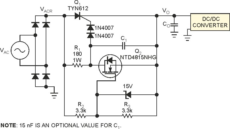
| Figure 1. | A thyristor and a MOSFET control current to bulk capacitor CO. This circuit limits the inrush current. |
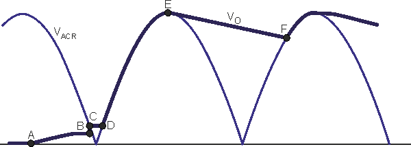
At turn-on, if the instantaneous rectified ac-line voltage, VACR, is greater than approximately 10 V, Point A in Figure 2, MOSFET Q2 turns on, forcing thyristor Q1 off. In this situation, a little current flows through R1 and Q2, injecting a small charge into bulk capacitor CO, Path A to B in Figure 2.
 |
|
| Figure 2. | If VACR is greater than approximately 10 V, MOSFET Q2 turns on; current flows through R1 and Q2, injecting a small charge into bulk capacitor CO. |
When VACR – VO ≤ 8 V or so, where VO is the output voltage, Q2 is off, letting Q1 conduct. In this situation, the bulk capacitor receives the necessary charge through Q1, Path B to C in Figure 2, to match VO to VACR. After this point, VACR falls below VO, and the bulk capacitor alone must support any power the dc/dc converter demands until VACR – VO ≥ 5 V or so, Path C to D in Figure 2. At Point D, VACR – VO ≈ 5 V and thyristor Q1 triggers, which conducts the capacitor’s charge current and the current the dc/dc converter demands until VACR matches the sinusoidal peak at Point E.
When VACR falls, thyristor Q1 cuts off, and the bulk capacitor alone feeds the dc/dc converter. The thyristor conducts again when VACR matches VO to the sinusoidal peak. This process then repeats. Use a nonsensitive gate thyristor with a breakdown voltage of at least 400 V for an ac voltage of 220 V rms (root mean square) and with twice the rms-current rating of the rectifier diodes.
This circuit uses a TYN610 thyristor. You can calculate the value of R1 using
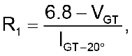
where VGT is the minimum gate-cathode voltage necessary to produce the gate-trigger current for Q1 and IGT–20° is the minimum gate current to trigger Q1 down to –20 °C. The NTD4815NHG MOSFET is suitable for this circuit. A MOSFET with a different threshold voltage may require different values for R2 and R3.
