Art Hogrefe
EDN
A number of circuits, such as level detectors and AM demodulators, benefit from a rectifier with a low offset voltage. Silicon diodes have an offset of approximately 0.6 V and do not work well in low-level circuitry. A Schottky diode is a bit better with an offset of approximately 0.4 V. A few germanium diodes are still available, but they do not tolerate the temperature range of silicon. Also, you can’t include a germanium diode in an IC. A superior configuration uses a bipolar transistor for these applications.
Figure 1 shows the bipolar-inverted-clamp circuit and a typical transfer function. The collector connects to ground or any other desired reference voltage. A fixed current drives the base. In the absence of any external drive, the emitter voltage is near zero. Driving the emitter with an external voltage produces the transfer function in Figure 1.
|
|||||
| Figure 1. | The bipolar inverted clamp (a) has an excellent rectification characteristic (b) because of the 2N3904’s large forward-beta-to-reverse-beta ratio. |
||||
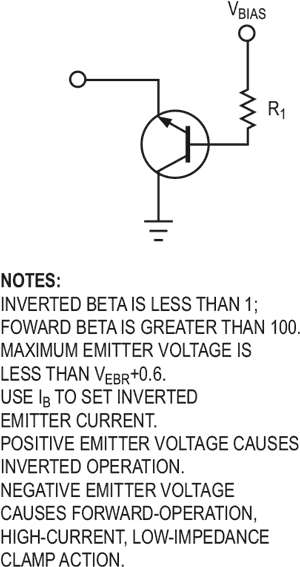
The circuit achieves this excellent rectification characteristic by using a transistor with a large forward-beta- to-reverse-beta ratio. Many of these transistors are still available. The 2N3904 provides excellent characteristics at a low cost. The reverse beta of the 2N3904 is only 0.25, so that for positive voltage on the emitter, and, with 40 µA of base drive, the emitter, current is around 10 µA. This current is sufficient in most level-detector applications for which the ac input amplitude changes slowly.
 |
|
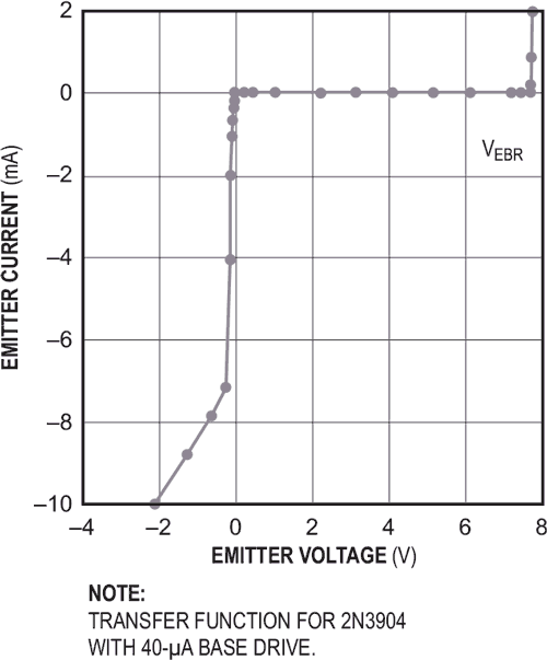
| Figure 2. | A logarithmic scale of the 2N3904’s forward-transistor emitter current and the forward current of the 1N34 show the impressive response of the 2N3904 at small voltages. |
The emitter current at even small negative voltages is much greater than in the inverted region because the forward beta of the 2N3904 is greater than 100. Impedance is low up to the beta-limited forward current, at which point the impedance increases to approximately the value of R1/beta. Figure 2 shows the forward-transistor emitter current of the 2N3904 and the forward current of the 1N34 germanium point-contact diode. The logarithmic current scale shows the impressive response of the 2N3904 at small voltages.
 |
|
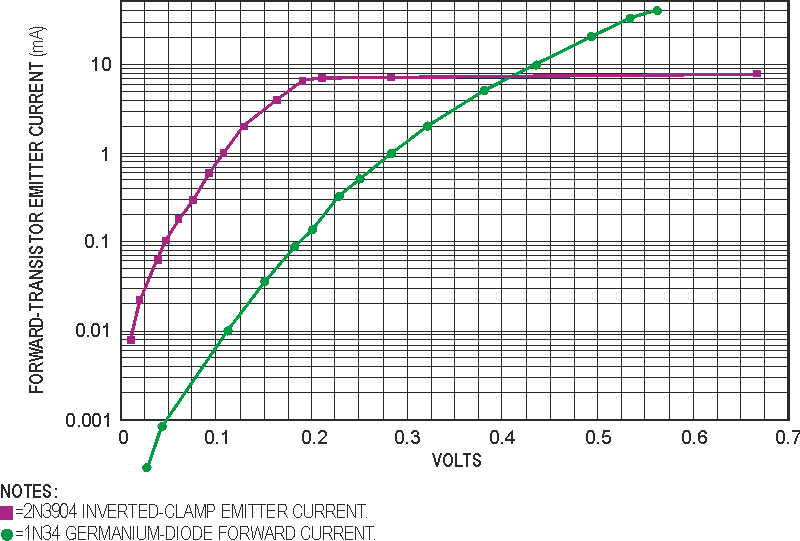
| Figure 3. | When operating as demodulators, the two configurations have similar input-level responses. |
Figure 3 shows the output as a level detector for the two clamps. The transistor circuit that produced these results is similar to the demodulator in Figure 4 except the base drive is 40 µA. For the 1N34, the anode connects to ground, and the cathode connects to the input capacitor in place of the transistor’s emitter. Figure 3 shows that the two configurations have similar responses to input levels and that the 2N3904 has a bit less offset, as you would expect from Figure 2. The output can drive a signal level meter or following electronics as part of an automatic-level-control or automatic-gain-control loop.
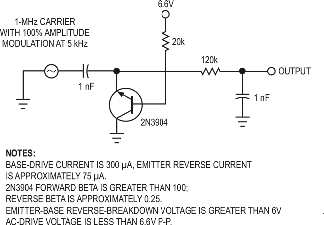 |
|
| Figure 4. | Using the inverted clamp as an AM demodulator requires a base current of 300 µA to track the RF-modulation envelope. |
The transfer function in Figure 1 also shows a sudden increase in inverted current at approximately 7.6 V, which occurs at the reverse breakdown voltage for the emitter-to-base junction. Because you know in this case that the base is near 0.6 V, the breakdown voltage for the tested part is near 7 V. Production circuits would have an input limit of 6.6 V p-p because of the minimum specified breakdown voltage of 6 V. Note that, for a small production, such as for test equipment, it is practical to select individual transistors to slightly increase the dynamic range. A 6 V p-p input dynamic range is sufficient in many applications.
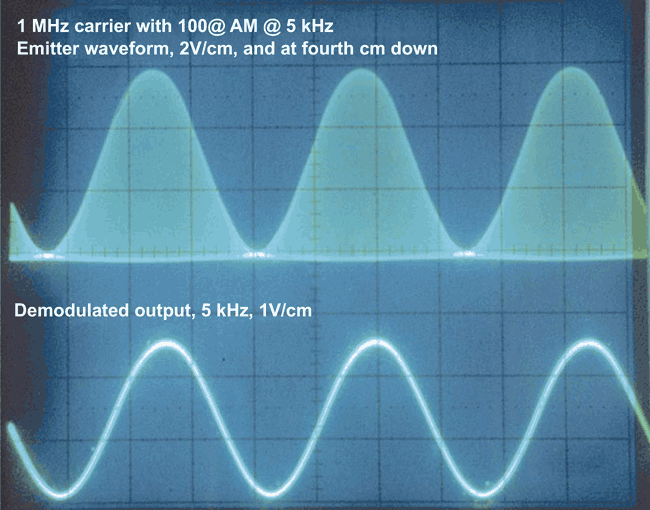 |
|
| Figure 5. | A scope photo shows the running demodulator; the upper trace is the emitter node, and the lower trace is the output. |
The RF demodulator in Figure 4 has a base drive current of 300 µA. This current is necessary to track the RF-modulation envelope and depends on the size of the input capacitor, modulation frequency, and maximum signal amplitude. The reverse current, which is IBASE times the reverse beta, must be large enough to discharge the input capacitor at the highest modulation frequency and amplitude to prevent distortion in the output waveform. Figure 5 shows the running demodulator with the upper trace at the emitter node and the lower trace at the output.
