Aaron Schultz, Linear Technology
Design Note 563
Introduction
A new family of op amps features industry leading speed versus supply current. The LTC6261/LTC6262/LTC6263 family (single, dual, quad) provides 30 MHz at a low 240 μA supply current, with 400 μV maximum offset voltage and rail-to-rail input and output. In combination with 1.8 V to 5.25 V supply, these op amps enable applications requiring uncompromised performance with low power and low voltage.
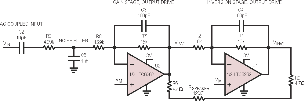
Bridge-Tied Differential Output Amplifier
The low supply current at the bandwidth and noise performance allows for excellent fidelity at a fraction of the usual dissipation in portable audio equipment. As with active filters, revisiting portable audio equipment headphone drivers is a rational enterprise, given the unique capabilities of the LTC6261.
Headphone speaker impedances range from 32 Ω to 300 Ω; their responsivity, from 80 dB to 100 dBSPL per 1 mW and beyond. As an example, considering a headphone speaker with 90 dBSPL per 1 mW, it takes 100 mW delivered to reach 110 dBSPL. With 32 Ω, the RMS current is 56 mA and voltage 1.8 V; with 120 Ω, 29 mA and 3.5 V.
Given a 3.3 V supply and the output of one LTC6261 amplifier, there may not be sufficient drive capability to yield 100 mW. However, the combination of two 180° phased amplifiers is enough to provide the necessary drive to reach upwards of 100 mW delivered power (Figure 1). Duplication of this bridge drive circuit enables power to both left and right sides.
 |
||
| Figure 1. | Audio Headphones Bridge Driver. | |
The LTC6263 provides four amplifiers in one small package. Data from a 2-amplifier LTC6262 driving what could be left or right is shown in Figures 2 and 3. Basic current consumption of the two amplifiers, with as much as 1 VP-P input but no load, is 500 μA.
 |
||
| Figure 2. | LTC6262 Bridge Driver THD and Noise with Different Loads vs Frequency. |
|
The circuit consists of first, an inverting gain stage with closed loop gain = 1.5, and a subsequent inverting stage. The combination of inverting stages produces a single-ended input to differential output gain of 3.
 |
||
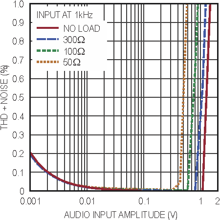
| Figure 3. | LTC6262 Bridge Driver THD and Noise with Different Loads vs Amplitude at 1 kHz. |
|
With 500 mVP-P input, the output is 1.5 VP-P, or 0.75 V max, or 0.53 VRMS. With 50 Ω, 500 mV input leads to approximately 5.6 mW delivered power. At 1 VP-P input, the circuit delivers 22.5 mW. Note that it helps that the LTC6261 output can swing close to rail-to-rail with load.
The first build of this circuit in the lab produced a significant tone at a few hundred Hz. It turned out that the positive input was not well grounded as an “AC ground” over all frequencies because the voltage was not strongly pegged. The need to peg the voltage arises when using a single supply rather than a dual supply. With a single supply, VM is not ground, but rather a mid-rail voltage created to enable inverting topologies to work properly. The resistor divider that creates VM has large resistance values (for example, two 470 k in series) to minimize additional supply current. A large capacitor ensures a strong ground at low frequencies. Indeed, the addition of a large capacitor (1 μF, which forms a pole with the 470 k resistors in parallel) eliminated the mysterious distortion tone.
Despite the low quiescent current, this driver delivers low distortion to a headphone load. At high enough amplitude, distortion increases dramatically as the op amp output clips. Clipping occurs sooner with more loading as the output transistors start to run out of current gain.
One significant concern in a portable device is battery drain. Music played loudly, or listeners’ musical choices affect the rate of battery drain. The end-use of a device is out of the designer’s control. Quiescent current, though, is not. Because much of a device’s time may be spent idle, quiescent current is significant, as it drains batteries continuously. The LTC6261’s low quiescent current increases battery discharge time.
Conclusion
The applications shown here take advantage of a unique combination of features available in the LTC6261 op amp family. The low quiescent current of these devices does not diminish their ability to perform at levels usually reserved for more power hungry parts. Rail-to-rail input and output, shutdown, and choice of package are features that add to their versatility.
