Aruna Rubasinghe
EDN
You can make a set/reset flip-flop from two NAND or NOR gates or use readily available set/reset flip-flop ICs, such as the 74HC279 quad-set/reset latch. The drawback of these methods is that they require a large amount of space to form the flip-flop. Even if you need only one flip-flop, you must use a large IC package with this approach. However, you can use a spare rail-to-rail op amp to perform the needed latch function (Figure 1).
 |
|
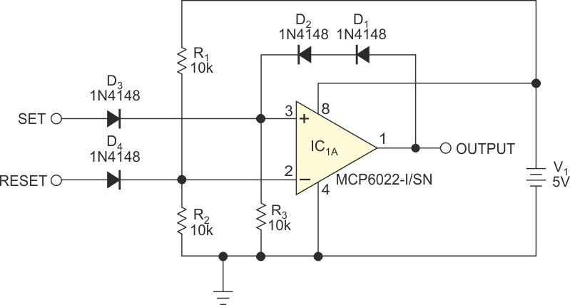
| Figure 1. | Positive feedback and diode steering latch the op amp’s output high or low when you apply a positive-going pulse to the set or the reset input. |
This approach has a low space requirement because the rail-to-rail-input/output MCP6022 is a dual-op-amp package, meaning that you can build two set/reset-latch circuits in a small amount of space. By choosing the appropriate op amp, you can also operate this circuit at nonstandard supply voltages if necessary.
You set the op amp’s inverting input to 2.5 V using the R1/R2 voltage divider. You cannot pull it lower than 2.5 V due to D4’s being reverse-biased. You can, however, drive the input to a logic high. Series diodes D1 and D2 apply positive feedback to the op amp’s noninverting input, which R3 pulls low if both the output and the set input are low.
With the output low, applying a 5 V pulse to the set input forward-biases D3; D1 and D2 remain reverse-biased. The resulting 4.4 V at the op amp’s noninverting input drives the output high, forward-biasing D1 and D2 and latching the noninverting input at 3.8 V – much higher than the inverting input voltage, even after the set input returns to low. If you then drive the reset input high, the inverting input, at 4.4 V, becomes higher than the noninverting input’s 3.8 V, driving the output low. When the reset input returns to low, D4 reverse-biases and the 2.5 V at the inverting input holds the output low. Note that the input pulses must be of sufficient duration to allow for the op amp’s delay and slew rate.
Unlike a true set/reset latch, both inputs’ being simultaneously active high yields unknown results. You can introduce a slight voltage offset by using a series resistor in either the set or the reset input to ensure a desired logic state under this condition. CMOS logic drives rail to rail and can interface directly with this circuit. However, driving with transistor-transistor logic requires pullup resistors at the TTL outputs to ensure sufficient input voltage. You may need to increase the value of the 10-kΩ resistors to avoid loading the pullup resistors.
The selected op amp must have rail-to-rail-output capability. You can use op amps without this ability by increasing the supply voltage as necessary to compensate the output voltage for the required logic level. You can change the trigger-voltage level by adjusting R1 and R2 and by using low-voltage drop diodes, such as germanium or Schottky types.
This circuit has relatively low input impedance, but it is usually not a problem because most logic-output signals can drive this load. You can change the input impedance by adjusting the resistor values as necessary.
