Praveen K
Electronic Design
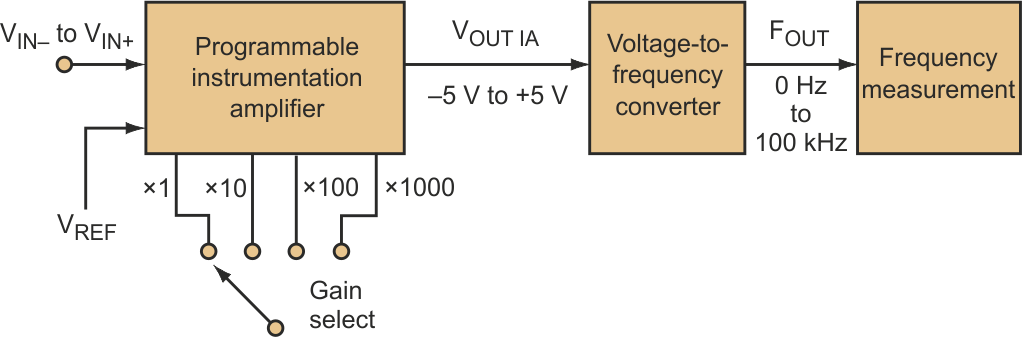
In certain applications, like pH measurement based on electromagnetic field (EMF) changes in an electrochemical reaction, the change in voltage is very small and the voltage range varies with the solution's concentration. Designers can make such microvolt measurements using a precision voltage-to-frequency converter (VFC) along with a programmable instrumentation amplifier (IA). The setup measures the voltage in terms of frequency and can measure microvolt changes for different ranges of voltages.
 |
||
| Figure 1. | Designers who need to make microvolt measurements can use an instrumentation amplifier and voltage-to-frequency converter in a relatively simple circuit. |
|
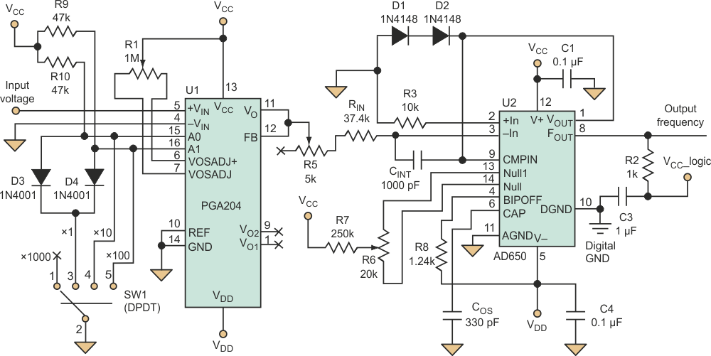
The circuit employs an AD650, high-precision VFC with a very low nonlinearity error of 0.002% at 10 kHz, 0.005% at 100 kHz, and 0.07% at 1 MHz (Fig. 1). The IA is a PGA204, a programmable-gain device whose gain can be digitally set to 1, 10, 100, or 1000. The PGA204 has a very low offset voltage of 50 µV and an offset voltage drift of 0.25 µV/°C. The input voltage is applied to the PGA204, which has an input impedance of the order 1010 Ω. The amplifier's output is:

In this circuit, the IA's VREF is grounded (Fig. 2).
 |
||
| Figure 2. | In this circuit, the output of the instrumentation amplifier should be between ±5 V since the voltage-to-frequency converter is configured for a bipolar input in that range. |
|
The VFC is designed for ±5-V operation, so the gain selected for the amplifier should reflect this limit and the input signal range. Variable resistor R1 allows offset adjustment.
With the AD650 configured in bipolar mode for an input signal range of ±5 V, the device provides a maximum output of 100 kHz. R2 is the pull-up resistor, which is chosen to limit the current through the output transistor to 8 mA. Input resistor RIN determines the input signal span, and timing capacitor COS determines the nonlinearity. Integration capacitor CINT is calculated as:

With an fMAX of 100 kHz, the minimum CINT is 1000 pF.
The components for the AD650 circuit should have very low temperature coefficients. The drift in input resistor RIN and in R3 and the timing capacitor COS directly affect the circuit's overall temperature stability. The temperature coefficient for R8 (1.24 kΩ) should match that of R3. The VFC's output, FOUT, varies linearly with VOUT IA:
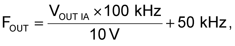
where 100 kHz is the maximum frequency output, 10 V is the maximum input voltage range, and 50 kHz is the frequency output at 0 V input.
| Table 1. | IA gain versus voltage range and resolution | ||||||||||||||||||||
|
|||||||||||||||||||||
Designers can select IA's gain to allow the VFC's FOUT to measure different input voltage ranges (see the Table 1). The circuit's measurement resolution (minimum measureable voltage) will also change accordingly. This circuit offers four major advantages:
- Processing becomes easier once the analog voltage is converted to the digital domain.
- The resolution is equivalent to a 17-bit analog-to-digital converter (ADC) for the 100-kHz operating range of the VFC.
- The circuit is so simple that the microvolt measurement can be performed with any frequency-measuring device.
- The VFC can also be designed for a 10-kHz or 1-MHz frequency range, depending on the resolution required.
