Michele Costantino
EDN
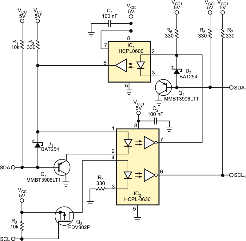
This Design Idea describes a simple and effective way to provide optoisolation for devices connected on the I2C bus (Figure 1). It improves on an earlier version (Reference 1). SDA and SCL are on the bus master’s side of the I2C bus; SDA1 and SCL1 are on the slave device’s side. It is fairly easy to optoisolate the clock line because it is unidirectional, from the master to the slave device. A P-channel MOSFET, Q3, provides the current for the LED of the fast optocoupler, IC2, buffering the clock line.
 |
||
| Figure 1. | This circuit provides an isolated, bidirectional, wired-OR connection of slave devices to the I2C-bus master. |
|
The data line, however, is bidirectional. This section of the circuit is symmetrical. Resistors R6 and R7 are the I2C pullup resistors on the slave device’s side of the bus, and R3 and R1 are dummy pullups in parallel with the main I2C pullup resistors on the SDA/SCL side. If both SDA and SDA1 lines are high – that is, no I2C devices are pulling them down – Q1 is off, no current flows into the LED of optocoupler IC2, IC2’s Pin 7 is high, Q2 is off, and the LED of optocoupler IC1 is also off.
If a device drives the SDA line low, Q1 and the LED of IC2 turn off, driving IC2’s Pin 7 low; diode D2 then starts to conduct. The result is a low level on the SDA1 line – the low output voltage of IC2 plus the threshold voltage of Schottky barrier diode D2. In this situation, it is important to notice that the LED of IC1 does not turn on because the voltage applied across it is below its threshold. This situation means that the circuit does not latch, and it can recover from this state once you release the SDA line.
Q3 and the PNP BJT (bipolar-junction transistor), Q1, effectively buffer the two SDA/SCL lines so that no extra current flows into the open-collector and -drain stages of the I2C devices that connect to the bus when they hold the lines down. This configuration allows the optoisolated interface to repeatedly pull low, providing wired-OR capability. Using Schottky barrier diodes for D1 and D2 rather than common diodes reduces the low-level voltage on the bus, improving the noise margin. Finally, because of the low propagation-delay times of the HCPL06XX devices that this design uses, this interface has no bus-glitch problems and works well at speeds of 400 kHz or higher (Reference 2).
