Glen Brisebois, Analog Devices
Design Note 399
Introduction
Photodiodes can be broken into two categories: large area photodiodes with their attendant high capacitance (30 pF to 3000 pF) and smaller area photodiodes with relatively low capacitance (10 pF or less). For optimal signal-to-noise performance, a transimpedance amplifier consisting of an inverting op amp and a feedback resistor is most commonly used to convert the photodiode current into voltage. In low noise amplifier design, large area photodiode amplifiers require more attention to reducing op amp input voltage noise, while small area photodiode amplifiers require more attention to reducing op amp input current noise and parasitic capacitances.
Small Area Photodiode Amplifiers
Small area photodiodes have very low capacitance, typically under 10 pF and some even below 1 pF. Their low capacitance makes them more approximate current sources to higher frequencies than large area photodiodes. One of the challenges of small area photodiode amplifier design is to maintain low input capacitance so that voltage noise does not become an issue and current noise dominates.
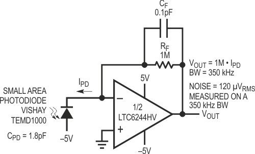
Figure 1 shows a simple small area photodiode amplifier using the LTC®6244. The input capacitance of the amplifier consists of CDM (the amplifier’s differential mode capacitance) and one CCM (the common mode capacitance at the amplifier’s – input only), or about 6 pF total. The small photodiode has 1.8 pF, so the input capacitance of the amplifier is dominating the capacitance. The small feedback capacitor is an actual component (AVX Accu-F series), but it is also in parallel with the op amp lead, resistor and parasitic capacitances, so the total real feedback capacitance is probably about 0.4 pF. This is important because feedback capacitance sets the compensation of the circuit and, with op amp gain bandwidth, the circuit bandwidth. This particular design has a bandwidth of 350 kHz, with an output noise of 120 μVRMS measured over that bandwidth.
 |
||
| Figure 1. | Transimpedance Amplifier for Small Area Photodiode. | |
Large Area Photodiode Amplifiers
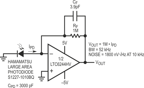
Figure 2a shows a simple large area photodiode amplifier. The capacitance of the photodiode is 3650 pF (nominally 3000 pF), and this has a significant effect on the noise performance of the circuit. For example, the photodiode capacitance at 10 kHz equates to an impedance of 4.36 kΩ, so the op amp circuit with 1 MΩ feedback has a noise gain of

at that frequency. Therefore, the LTC6244 input voltage noise gets to the output as
NG × 7.8 nV/√Hz = 1800 nV/√Hz,
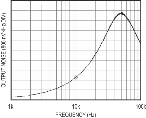
and this can clearly be seen in the circuit’s output noise spectrum in Figure 2b. Note that we have not yet accounted for the op amp current noise, or for the 130 nV/√Hz of the gain resistor, but these are obviously trivial compared to the op amp voltage noise and the noise gain. For reference, the DC output offset of this circuit is about 100 μV, bandwidth is 52 kHz, and the total noise was measured at 1.7 mVRMS on a 100 kHz measurement bandwidth.
 |
||
| Figure 2a. | Large Area Photodiode Transimpedance Amp. | |
 |
||
| Figure 2b. | Output Noise Spectral Density of the Circuit of Figure 2a. At 10 kHz, the 1800 nV/√Hz Output Noise is Due Almost Entirely to the 7.8 nV Voltage Noise of the LTC6244 and the High Noise Gain of the 1 M Feedback Resistor Looking into the High Photodiode Capacitance. |
|
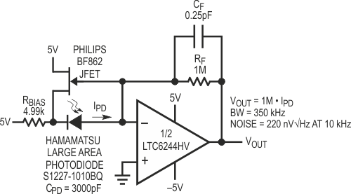
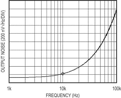
An improvement to this circuit is shown in Figure 3a, where the large diode capacitance is bootstrapped by a 1 nV/√Hz JFET. This depletion JFET has a VGS of about –0.5 V, so that RBIAS forces it to operate at just over 1 mA of drain current. Connected as shown, the photodiode has a reverse bias of one VGS, so its capacitance will be slightly lower than in the previous case (measured 2640 pF), but the most drastic effects are due to the bootstrapping. Figure 3b shows the output noise of the new circuit. Noise at 10 kHz is now 220 nV/√Hz, and the 130 nV/√Hz noise thermal noise floor of the 1 M feedback resistor is discernible at low frequencies. What has happened is that the 7.8 nV/√Hz of the op amp has been effectively replaced by the 1 nV/√Hz of the JFET. This is because the 1 M feedback resistor is no longer “looking back” into the large photodiode capacitance. It is instead looking back into a JFET gate capacitance, an op amp input capacitance, and some parasitics, approximately 10 pF total. The large photodiode capacitance is across the gate-source voltage of the low noise JFET. Doing a sample calculation at 10 kHz as before, the photodiode capacitance looks like 6 kΩ, so the 1 nV/√Hz of the JFET creates a current noise of 1 nV/6 k = 167 fA/√Hz.
 |
||
| Figure 3a. | Large Area Diode Bootstrapping. | |
 |
||
| Figure 3b. | Output Noise Spectral Density of Figure 3a. The Simple JFET Bootstrap Improves Noise (and Bandwidth) Drastically. Noise Density at 10 kHz is Now 220 nV/√Hz, About an 8.2x Reduction. This is Mostly Due to the Bootstrap Effect of Swapping the 1 nV/√Hz of the JFET for the 7.8 nV/√Hz of the Op Amp. |
|
This current noise necessarily flows through the 1 M feedback resistor, and so appears as 167 nV/√Hz at the output. Adding the 130 nV/√Hz of the resistor (RMS wise) gives a total calculated noise density of 210 nV/√Hz, agreeing well with the measured noise of Figure 3b. Another drastic improvement is in bandwidth, now over 350 kHz, as the bootstrap enabled a reduction of the compensating feedback capacitance. Note that the bootstrap does not affect the DC accuracy of the amplifier, except by adding a few picoamps of gate current.
