James Mahoney
EDN
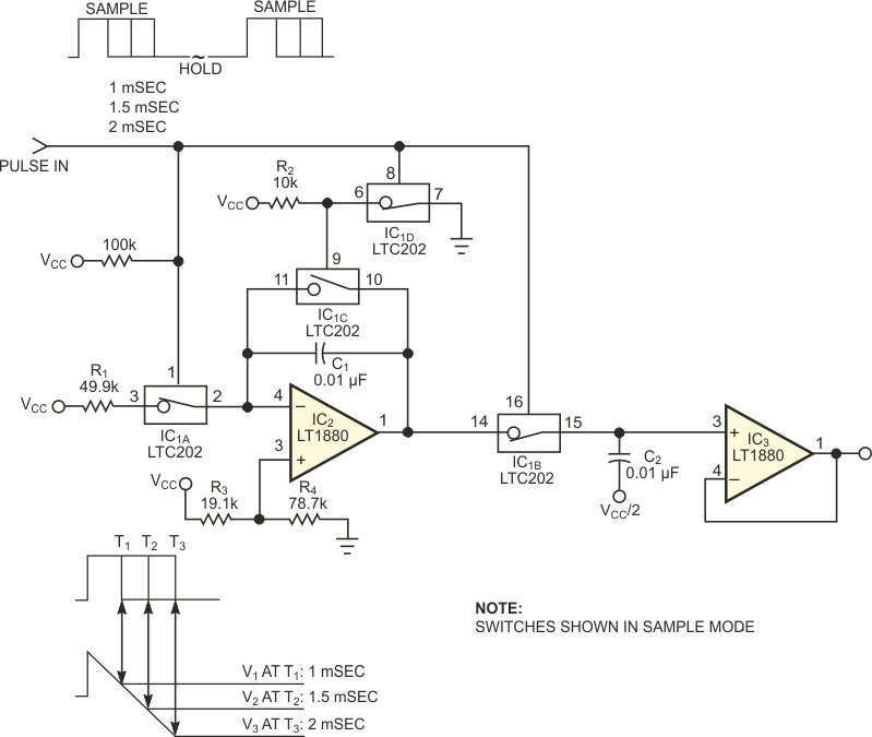
The circuit in Figure 1 converts pulse information to a clean dc voltage by the end of a single incoming pulse. In another technique, an RC filter can convert a PWM signal to an averaged dc voltage, but this method is slow in responding. Converting low-duty-cycle pulse information is slower yet. The circuit in Figure 1 uses two low-input-bias-current LT1880 op amps, IC2 and IC3, and an LTC202 quad analog switch, IC1A, IC1B, IC1C, and IC1D, to configure the integrator and sample-and-hold stages that convert a single pulse to a dc voltage. The circuit's output is stable after a single pulse. This example shows the conversion of a low-duty-cycle positive pulse, whose width varies from 1 to 2 msec with a period of 25 msec, to a clean dc voltage. The input pulse starts, stops, and resets the integrator and controls the input to the sample-and-hold stage. After the reset operation, the positive pulse level-triggers the integrator, comprising R1, C1, and IC2. The sample-and-hold stage, comprising IC1B, C2, and IC3, is in the sample mode, sampling the output of the integrator, while the incoming pulse is high.
 |
||
| Figure 1. | This circuit yields a clean dc voltage that indicates the width of an incoming pulse. | |
When the incoming pulse goes low, the circuit disconnects the input to the sample-and-hold stage, putting it into hold mode. The integrator then stays in the reset state until the next positive pulse arrives. During reset, analog switch IC1A opens to disconnect the integrator's input, switch IC1C closes to reset integration capacitor C1, and switch IC1B opens to disconnect the input to the sample-and-hold stage, placing the stage in hold mode. Analog switch IC1D inverts the on/off states of switch IC1C. The LT1880 op amp is a good choice for the integrator and sample-and-hold stages because of its maximum input-bias current of 900 pA at 25°C and maximum of 1500 pA maximum over the full –40 to +85 °C ambient-temperature range. Another benefit of the LT1880 is its maximum input-offset-voltage drift of 1.2 µV/°C. Integrator capacitor and resistor R1 set the conversion gain.
 |
||
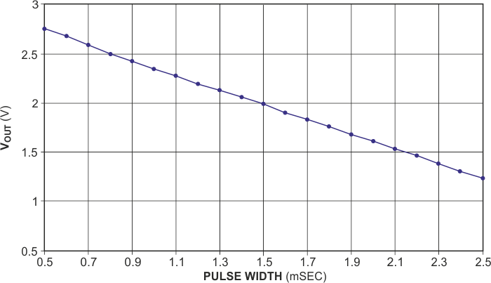
| Figure 2. | The circuit in Figure 1 linearly converts a pulse width to a dc voltage. | |
You should use polypropylene, polystyrene, or Teflon capacitors for C1 and C2 to minimize integrator drift and sample-and-hold droop rate. The voltage ratio that resistors R3 and R4 set establishes the dc level at the positive pulse's midrange value: 1.5 msec in this example. Figure 2 shows input pulse width versus output voltage. You can easily modify the circuit in Figure 1 to yield different conversion gains, output levels, and swings for different pulse widths. The circuit operates with pulse-width information and not duty-cycle values. The sample-and-hold stage is an analog-memory element that reveals the dc-voltage equivalent for this pulse width.
