Tom Gross, Linear Technology
EDN
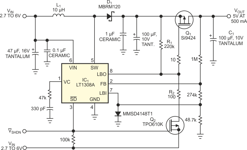
The SEPIC (single-ended, primary-inductance-converter) topology is generally a good choice for voltage regulators that must produce an on output voltage that falls in the middle of the input-voltage range, such as a 5 V output from a 2.7 to 6 V input. The topology has some disadvantages, however. The efficiency of a SEPIC circuit fares worse than that of buck and boost regulators, and SEPIC designs often involve the use of large, complex magnetic components, thereby complicating the design task. Figure 1 shows a simple and efficient alternative topology. When the input voltage is lower than the output voltage, the circuit operates as a normal boost regulator. The inductor, L1, stores energy when switch Q1 is on and the boost diode, D1, is reverse-biased. While D1 is off, the output capacitor, C1, delivers the load current. When Q1 turns off, L1 reverses its polarity, thereby forward-biasing D1. L1 then charges C1 and delivers current to the load. The inductor voltage adds to the input voltage to generate the output voltage.
 |
||
| Figure 1. | This circuit can both boost and step down the input voltage, depending on whether the input voltage is lower or higher than the output voltage. |
|
The low-battery comparator in IC1, which usually checks battery levels, monitors the output voltage through its LBI pin. IC1's internal comparator output switches low (sinking current). This action turns the p-channel Q1 fully on, creating a low-impedance path to the output. When the input voltage is the same value as or greater than the output voltage, the circuit functions like a linear regulator. In this case, the internal comparator's output assumes a high-impedance state. The voltage at the gate of Q1 begins to pull up through R1, a 220-kΩ resistor, so Q1 begins to turn off. This action forces the output voltage to decrease, and the comparator eventually again switches states from high to low (sinking current). The comparator's low state causes the output voltage to rise again, and the cycle repeats. Thus, the circuit begins to operate as a linear regulator, with Q1 acting as the pass transistor.
 |
||
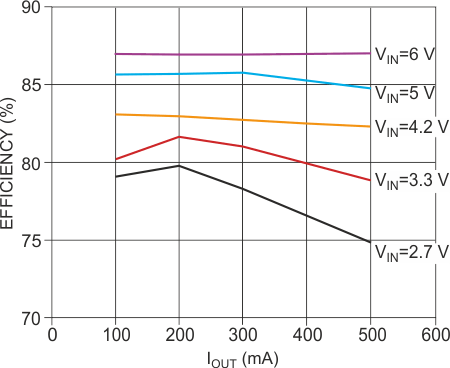
| Figure 2. | The efficiency of the circuit in Figure 1 depends on whether the circuit acts as a boost converter or a linear regulator. |
|
The circuit can also disconnect the input-to-output current path, unlike a conventional boost regulator. The shutdown signal (/VSHDN) connects to the gate of Q2, a logic-level, p-channel MOSFET, as well as to IC1's shutdown (/SD) pin. When the shutdown signal goes low, it turns off IC1 and turns on Q2. This action delivers VIN (via R2, a 100 Ω resistor) to the gate of Q1, thereby turning off the transistor. Hence, the shutdown operation disconnects the input-to-output current path. Figure 2 shows how the efficiency of this linear-boost regulator depends on its mode of operation. When the input voltage is lower than the output voltage, the efficiency of the regulator is that of a boost regulator. When the input voltage exceeds the output voltage, the circuit operates as a linear regulator in which efficiency is approximately VOUT/VIN.
