Henry Santana
Electronic Design Europe
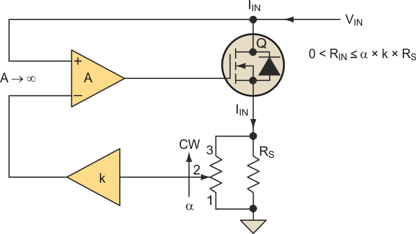
The general approach to an electronic load is to use a transistor across the input terminals so the current flows from drain (collector) to source (emitter). A resistance is effected by causing a current flow in proportion to the applied voltage in the manner of a resistor, I = V/R. A controller monitors the applied voltage and adjusts the current in response (Fig. 1).
 |
||
| Figure 1. | An electronic load typically employs a transistor across the input terminals so the current flows from drain (collector) to source (emitter). |
|
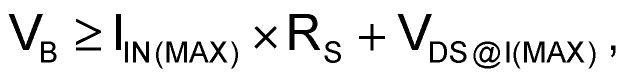
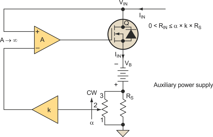
To achieve 0 Ω, the terminal voltage must be 0 in the presence of a current. Under this condition the pass transistor suffers a loss of operating voltage and cannot conduct a current. To maintain conduction of the pass transistor, an auxiliary power supply is connected (Fig. 2). The required voltage,
is sufficient to maintain forward conduction with VIN = 0 and 0 < IIN ≤ IIN(MAX). This condition corresponds to an effective zero input resistance.
It can be shown that
RIN = α × k × RS
for 0 ≤ α ≤ 1 and where k multiplies RS so it can be made small to reduce power loss. If, for example, RS = 1.0 Ω, k = 100, then 0 ≤ RIN ≤ 100 Ω for 0 ≤ α ≤ 1. If IIN(MAX) = 1 A and VDS@I(MAX) = 2 V, then VB ≥ 3 V.
In virtually all applications, the pass transistor must be heatsinked as the power dissipated is
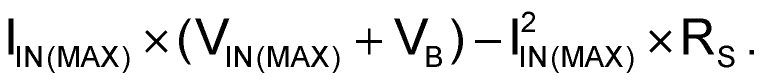
If in this example VIN(MAX) = 15 V, the pass transistor would have a maximum dissipation of 17 W. This would appear as a 15-W resistor adjustable over 0 to 100 Ω.
You may be wondering why an additional power source was introduced between the source of the MOSFET and the current sense resistor to achieve a “0-Ω load” condition (essentially a short across input voltage) in Figure 2. After all, why would you need an electronic load that can go down to 0 V (i.e., short circuit) condition?
 |
||
| Figure 2. | To maintain conduction of the pass transistor for a zero-load condition, the circuit uses an auxiliary power supply. |
|
If you wanted to short an electronic load, you could always use a relay directly across the input voltage. Or if you wanted it to be all solid state, you could place another MOSFET that has much higher current capacity (and very low RDS(on) that approaches a few milliohms) directly across the input and turn it on using a switch. This approach would be much simpler (and cost effective) than adding a second power supply in series with sense resistor. So, why would you use the additional power source?
Here’s the answer. This electronic load can check low-voltage power supplies (i.e., 3.3 V and lower) where a voltage burden (i.e., 1 V) would not permit testing under short-circuit condition. This is useful in testing the short-circuit response of power supplies, current trip level, and effectiveness of overload protection.
Furthermore, even with a low RDS(ON), a MOSFET will not conduct at 0 V (VDS). At high currents, a MOSFET requires non-zero voltage (see note A) to sustain conduction. This circuit will maintain VDS right into a virtual short circuit.
Finally, a hard switch such as a relay does not permit a smooth transition of resistance. The circuit described here acts more like a rheostat but with the ability to be voltage controlled (see note B) from a remote point. The controller does not have to carry the load current. It would require multiple relays to apply a range of loading. This circuit can provide smooth (stepless) effective resistive loading over a large range including 0 Ω.
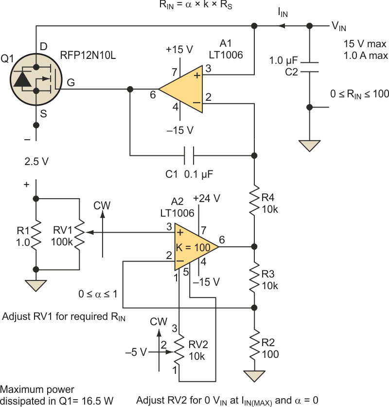 |
||
| Figure 3. | An application circuit like this one achieves a zero-load condition for testing low-voltage power supplies. |
|
The circuit can be scaled up to higher voltages and currents. Figure 3 shows an application.
Note A:
For example, an RFP30N06 MOSFET has a specified RDS(on) of 0.047 Ω. At 30 A this device requires at least 2 V VDS. This would not be an effective short circuit on a 3.3-V, 30-A power supply. On a 1.8-V supply, it would not conduct this current.
Note B:
The effective resistance can be controlled with a voltage-controlled amplifier [1].
