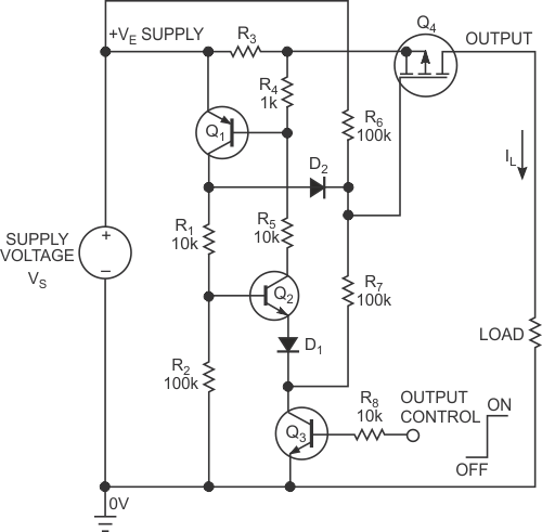
The circuit in Figure 1 lets you switch high-voltage power to a grounded load with a low-voltage control signal. The circuit also functions as a submicrosecond circuit breaker that protects the power source against load faults. Power switches to the load when you apply a logic-level signal to the output control terminal. When the signal is lower than 0.7 V, transistor Q3 is off and the gate of P-channel MOSFET Q4 pulls up to the positive supply through R6, thus holding Q4 off. During this off condition, the circuit’s quiescent-current drain is 0 A.
 |
||
| Figure 1. | This inexpensive power switch incorporates a submicrosecond circuit breaker. | |
A 3 to 5 V signal at the control terminal turns on Q3, which pulls R7 to 0 V, providing gate drive for Q4. The MOSFET now turns on and sources the load current, IL, through sense resistor R3 to the load. If R3’s and Q4’s on-resistances are smaller than the load resistance, the magnitude of the supply voltage, VS, and the load resistance mainly determine the load current.
Under normal load conditions, the sense voltage developed across R3 is too small to bias Q1 on; thus, Q1 and Q2 are both off. If, however, the load current increases, the voltage across R3 may become large enough to turn on Q1. At that point, base current flows through R4 to Q1, and Q1’s collector current in turn provides base current for Q2. As Q2 turns on, it provides extra base drive for Q1, and the two transistors rapidly latch in the on-state.
With Q1 saturated, its collector pulls D2’s anode to the positive supply, which clamps Q4’s gate voltage to a diode drop below VS. Without gate drive, the MOSFET turns off, and IL falls to 0 A. With Q1 and Q2 both latched on, Q4 remains off, which protects the power source from excessive load currents. You can reset the circuit breaker simply by taking the control signal low or by cycling the power. The resistance values in Figure 1 are suitable for operation at supply voltages of 20 to 30 V. Assuming that the transistors are suitably rated, the circuit can operate at much higher voltages, but you must scale the resistor values accordingly. Operation at a voltage as low as approximately 5 V is also possible, but you may need to reduce the values of R1 and R5 to ensure proper drive for Q1 and Q2. Resistors R6 and R7 form a potential divider, which sets Q4’s gate-to-source voltage, VGS, to a value large enough to enhance the MOSFET fully when Q3 is turned on.
At low supply voltages, you may need to change the ratio of R6 to R7 to ensure that the gate-to-source voltage is large enough to provide adequate gate drive for Q4. When the circuit is operating at high voltages, you may need small-signal diode D1 to prevent reverse avalanche breakdown of Q2’s base-to-emitter junction when Q3 is off. However, you can omit D1 at low supply voltages, which are too small to cause avalanche breakdown.
When selecting components, choose high-gain devices for the bipolar transistors and ensure that D2 has low reverse-leakage current; avoid using a Schottky diode. In the off-state, each transistor has the full supply voltage across its collector-to-emitter or drain-to-source terminals, so ensure the maximum voltage ratings across these terminals are greater than the maximum supply voltage.
The circuit breaker trips at a load-current threshold:
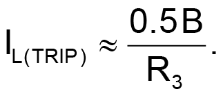
For example, with a supply voltage of 24 V and with R3 having a value of 6.8 Ω, a test circuit using the values in Figure 1 trips at a load current of 80 mA. The actual trip point varies slightly with temperature and depends on the device you use for Q1, so be prepared to adjust the value of R3 to achieve the desired trip current.
In addition to providing a latching function, the positive feedback loop around Q1 and Q2 ensures that the circuit breaker responds quickly to an overload current. The actual trip time depends somewhat on the magnitude of the fault current. With a supply voltage of 24 V and with R3 having a value of 6.8 Ω, the test circuit takes 6 µsec to trip at a fault current of 80 mA. However, increasing the fault current to 200 mA results in a trip time of just 500 nsec.
Capacitive loads, filament bulbs, and motors exhibit a large inrush current and could cause the circuit breaker to trip when the control signal goes high even though the normal, steady-state load current is below the trip threshold. If this scenario is likely to be a problem, consider connecting R7 to a separate transistor so that you can independently control the circuit breaker and the power switch. This approach lets inrush current subside before enabling the circuit breaker.
