Ramachandra Mutagi
EDN
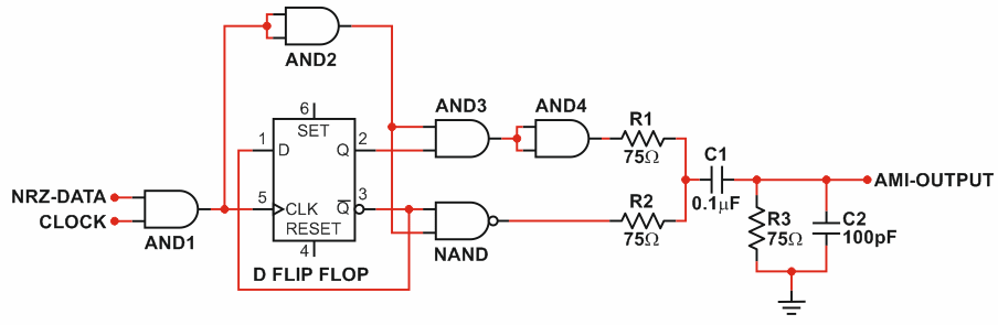
Alternate mark inversion (AMI) coding is often used in digital data trasnmission over cables as it has no DC component. Besides, the bandwidth of an AMI signal is lower than the equivalent return-to-zero (RZ) format. Normally, to generate a bipolar waveform such as AMI, one needs positive and negative supplies. Also, the circuit will likely employ analog components for bipolar waveform generation. However, this Design Idea eliminates all these requirements and generates an AMI waveform from an NRZ input using only a few gates, a flip-flop, and a single 5 V supply.
 |
|
| Figure 1. | The NRZ to AMI converter generating bipolar pulses uses single supply. |
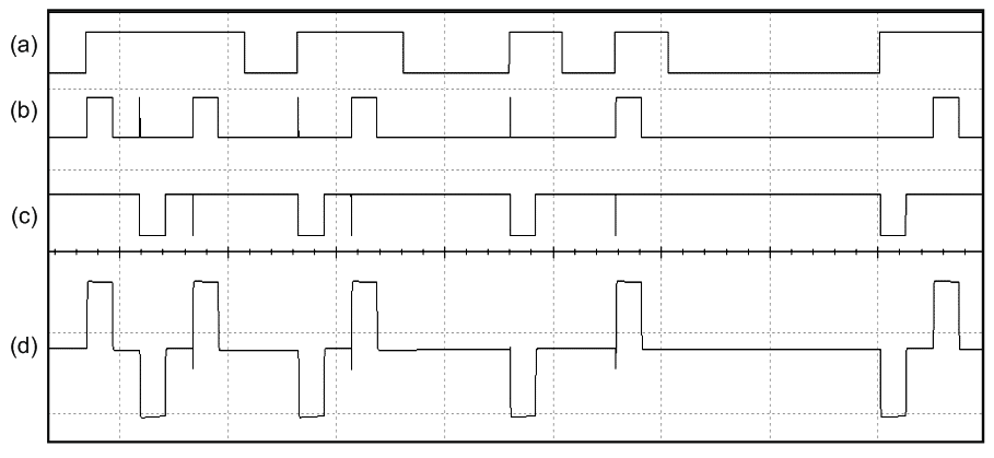
Refering to Figure 1, the NRZ signal (Figure 2a) is gated with the clock using the AND1 gate, generating an RZ waveform (Figure 2b). The RZ signal clocks a D-FF connected as a frequency divider. The RZ signal is then gated with the Q and /Q outputs of the flip-flop, separating alternating pulses on two lines at the outputs of the AND2 and NAND gates. The NAND gate is used on the second line to obtain an inverted waveform (Figure 2c).
 |
|
| Figure 2. | The waveforms: (a) NRZ input; (b) clock gated RZ output at AND1; (c) NAND output; (d) AMI output. |
Since the delay of the NAND is more than the AND gate, AND4 is used at the output of AND3 to compensate (this can be changed depending on the logic family used). The outputs of the AND4 and NAND gates drive 75 Ω resistors which effectively add the voltages at the gate outputs. If both the outputs are high, the voltage at the junction of the resistors is a high level. If one of the outputs is low and other high, the voltage at the junction is half the high level voltage. When both outputs are low, the voltage at the junction is close to 0 V. Thus, the waveform at the junction of R1 and R2 shows positive and negative pulses around a DC level. This signal passes through DC block C1, and we get a true bipolar waveform with zero DC level at the output (Figure 2d).
Figure 2 shows waveforms of the simulated circuit. The simulator does capture very small spikes appearing at the gate outputs, which will not cause problems in real use. The NRZ signal was generated at 2.048 Mb/s. Because of the TTL devices and 5 V supply, the peak-peak signal level is less than ±2.5 V. If higher amplitude is needed, CMOS devices with higher logic swings may be used.