This board is a Microchip PIC prototyping board for the 18F4550 microcontroller using USB. It is designed to have the PIC loaded with a USB bootloader and then a separate programmer is no longer needed. The board has all the circuitry needed for a successful USB interface. Free I/O pins have 1-3 solder pads for easy connection for prototyping. This board is based on the one I use for all my own USB experimentation, and is compatible with the firmware and software in my 18F4550 USB Interface article, my PIC USB Bootloader article, and others. It should also work fine for other PIC USB interfacing projects, such as HID or CDC (virtual COM port) applications.
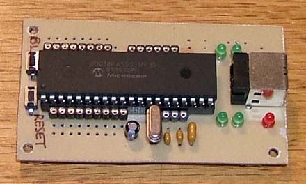
This is a rough idea of what the board will look like - a picture of the first revision of this board, homemade, which I currently use.

Download the Schematic and PCB Layout Files (Eagle 4.16 Format)
The board can be populated with a 7805 voltage regulator for use with an external power supply, or can be used directly from USB bus power (up to the current limit of USB), with a 3-pin header that can be used with a jumper to select one mode or the other. The board is made with a mixture of through-hole and surface-mount components, however all of the surface-mount components are resistors or capacitors (only 2 leads), and are the 1206 package size (not microscopic), which are not very hard to solder successfully.
| Capacitors | |||
| Value | Qty | Description | Digikey part no. |
| 22 pF | 2 | Radial leaded ceramic | BC1034CT-ND |
| 0.1 uF | 3 | 1206 SMD ceramic | 399-1249-1-ND |
| 0.47 uF | 1 | Radial leaded ceramic | 399-4299-ND |
| 1 uF | 2 | Electrolytic, 50 v, 5 mm diameter | P13460-ND |
| Resistors | |||
| Value | Qty | Description | Digikey part no. |
| 1 k | 5 | 1206 SMD | P1.0KECT-ND |
| 10 k | 2 | 1206 SMD | P10KECT-ND |
| Misc | |||
| Name | Qty | Description | Digikey part no. |
| PIC | 1 | 18F4550-I/P | PIC18F4550-I/P-ND |
| Crystal | 1 | 20 MHz | X439-ND |
| LED | 4 | Green, 3mm | 160-1144-ND |
| LED | 1 | Red, 3 mm | 160-1667-ND |
| USB Jack | 1 | 609-1039-ND | |
| Vreg | 1 | 7805 5 V regulator | LM7805CT-ND |
| Pushbuttons | 2 | P8057S-ND | |
| 2 pin header | 2 | Can cut from larger snappable header | WM8072-ND |
| 3 pin header | 1 | Can cut from larger snappable header | WM8073-ND |
| IC Socket | 1 | 40-pin DIP | AE8940-ND |
| shunt | 1 | 2-pin shorting jumper | A26228-ND |
| SIP sockets | 1 | 36-pin snappable SIP socket (optional) | 929974-01-36-ND |
Assembly Instructions
Note: these instructions assume that the user has moderate soldering skills, at least with through-hole components.The exact order of assembly isn't really important, I'm just listing it in the usual order of shortest to tallest components, roughly.
- It is probably best to start by soldering all of the surface-mount parts first. There are 3 capacitors and 7 resistors. None of them are polarized, so don't worry about which direction you solder them on. Probably the easiest method for soldering these parts is as follows:
-Place a small blob of solder on one of the two pads on the board
-Pick up the part with a pair of needle nose pliers or tweezers.
-Hold the part over the pads with one hand, so it is resting on the solder blob.
-With the other hand, gently tap the solder end of it so that the solder melts and bonds the part.
-Remove the tweezers/pliers, and apply solder to the other end of the part to solder it to the other pad.
-Go back and touch up the first pad with a little more solder, for a cleaner joint, if needed.
It may sound like a lot, but it really only takes a few seconds per part. (you can omit C8 if you don't want to populate the voltage regulator - see more info further down) - Solder in the IC socket. Because of its size, it may be helpful to use a piece of tape to hold it in place while you flip the board and solder it. It's also a good idea to solder just two pins in opposite corners to hold it in place, flip the board back to make sure it's fully seated and flat with respect to the board, before soldering the rest of the pins. If not, just heat the solder joints again while pressing the socket in from the other side.
- Solder in the pushbutton switches.
- Solder in the ceramic capacitors C1-C3. These are non-polarized so orientation doesn't matter.
- Solder in the crystal. Again, orientation doesn't matter here.
- Solder in the LEDs. LED1-LED4 are green, and in case the orientation on the board isn't clear, the flat sides should be facing out from the center of the board - LED1&2 facing the Hack A Day logo, LED3&4 facing the other way. LED5 is red, and the flat should be facing down, toward the USB connector.
- Solder in the electrolytic capacitor C5. Pay attention to orientation, the negative side should be toward the bottom edge of the board, with the logos.
- Solder in the USB connector.
- (Optional) Solder SIP sockets into one row of the prototyping pads. These sockets come in a longer strip, and can be snapped to whatever length you need. Since the prototyping pads don't include all pins, you need to snap the headers into several smaller pieces. It is helpful to use some tape to hold the headers in position (and upright) while soldering.
- Solder jumpers J1 (3-pin), J2 and J3 (2-pin).
- Solder in the 5V regulator, IC1. The heatsink side of the case should be facing the top edge of the board, away from the IC socket.
- Solder in the electrolytic capacitor, C7. Negative lead should be facing the IC socket.
At this point you should be done with the basic assembly! You can program the PIC with a bootloader or other firmware using a traditional PIC programmer, stick it in the socket, and be ready to go. The SIP sockets are handy because you can simply insert wires to run connections to a breadboard, etc.
As for the jumpers: J1 allows you to select between external power via the voltage regulator, and USB bus power. Place one of the 2-pin shorting jumpers on it. These are the same thing used for jumper settings on hard drives, CDROM drives, motherboards, etc., so feel free to steal one from some old computer equipment instead of buying some. J2 is for external power to the voltage regulator, from a 9 v battery or whatever you choose to use. See the 7805 datasheet for acceptable input voltage ranges. J3 is for running power to your breadboard or other external board if you want, or it could also be used to power this board from an existing external regulated 5 v supply.
