Luca Bruno
EDN
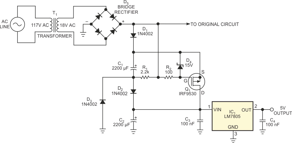
You can use the circuit in Figure 1 to obtain a low regulated voltage, such as 5 V dc, from a higher voltage, rectified, sinusoidal voltage source without resorting to an electrically noisy dc/dc converter or wasting watts in a dropping resistor. This application requires a regulated 5 V-dc source, but a transformer supplies 18 V rms to a full-wave bridge rectifier.
 |
||
| Figure 1. | In this unconventional step-down circuit, capacitors C1 and C2 charge in series and discharge in parallel, reducing the voltage applied to regulator IC1. |
|
During the charging phase, two equal-value electrolytic capacitors, C1 and C2, receive charging current when connected in series through forward-biased diodes D1 and D2. An enhancement P-channel MOSFET transistor, Q1, an International Rectifier IRF9530, remains off because its gate receives a slightly positive reverse-gate-bias voltage due to zener diode D4's forward-voltage drop. Each capacitor charges to approximately one-half the peak value of the rectified voltage minus the forward-voltage drops that D1 and D2 present. The full-wave bridge rectifier, D5, or Graetz bridge, produces these drops.
When the discharge phase begins, D1 gets reverse-biased, and capacitor C2 discharges through the load that voltage regulator IC1 presents. Subsequently, the anode voltage of diode D1 continues to decrease, Q1's gate-to-source voltage becomes negative, and the transistor conducts, allowing C1 to discharge into the load through forward-biased diode D3. In effect, the two capacitors charge in series and discharge in parallel into the load, halving the raw rectified voltage and ripple voltage at IC1's input. During C1's discharge, zener diode D4 protects Q1 by clamping its gate-to-source voltage within its maximum rating.
To function properly, the circuit requires a minimum load current; the regulator's quiescent-current drain is usually enough. Otherwise, capacitor C2 charges to the peak voltage available from D5. The values of C1 and C2 and the ratings of the remaining components depend on the maximum load current required. The values of resistors R1 and R2 are not critical. Note that Q1 functions as a switch; selecting a device with low on-resistance limits Q1's power dissipation.
