Guy Hoover, Analog Devices
Design Note 568
Attaining optimal SNR performance from an ADC isn’t just a matter of providing a low noise signal to the ADC’s input. Providing a low noise reference voltage is just as important. While reference noise has no effect at zero-scale, at full-scale any noise on the reference will be visible in the output code. This is why dynamic range (DR) which is measured at zero-scale is usually several dB better for a given ADC than the signal-to-noise ratio (SNR) which is measured at or near full-scale. Providing a low noise reference voltage is particularly important in an oversampling application where it’s possible for the ADC’s SNR to exceed 140 dB. To achieve an SNR at this level, even the best low noise references need some help to reduce their noise levels.
There are several alternatives that can reduce reference noise. Increasing the size of the bypass capacitor or using a simple lowpass RC filter on the reference output are not good alternatives. A large bypass capacitor on the reference output by itself cannot produce a low enough cutoff frequency to be effective. A passive RC filter by itself, while providing a low cutoff frequency, will produce an output voltage that varies with sampling frequency and temperature. Paralleling the outputs of multiple low noise references is an effective alternative, but it is expensive and consumes a lot of power.
The reference filter demonstrated here produces a low noise reference voltage without significantly compromising the reference accuracy or temperature coefficient and does so with only moderate power consumption and cost.
Circuit Description
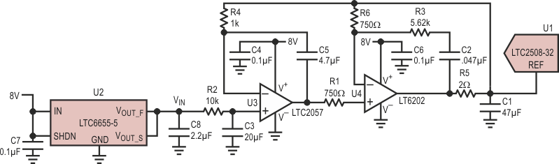
The ADC used in this example is the LTC2508-32 (U1). The LTC2508-32 is a low noise, low power, 32-bit SAR ADC with a lowpass digital filter that has four pin-selectable downsampling factors (DF) ranging from 256 to 16384. A low noise, low temperature drift reference is necessary to achieve the full performance of the LTC2508-32.
The reference used in this example is the LTC6655-5 (U2). The LTC6655-5 offers high accuracy (±0.025% Max), exceptionally low noise (0.67 ppm RMS Typ) and drift (2 ppm/°C Max) performance. Even with its exceptionally low noise performance, the LTC6655-5 still degrades the SNR performance of the LTC2508-32.
The LTC2057 (U3) is a zero-drift op amp that has suppressed 1/f noise. The LTC2057 has an input bias current (IB) of less than 200 pA, a maximum offset voltage of 4 μV and a maximum offset voltage temperature coefficient of 0.015 μV/°C. This is significantly lower than the temperature coefficient of the LTC6655-5 (2 ppm/°C = 10 μV/°C).
The LT6202 (U4) is a low noise, fast settling op amp with the high short-circuit current capability necessary to drive the 47 μF bypass capacitor required on the REF pin of the LTC2508-32.
The circuit of Figure 1 filters the output of reference (U2) using R2 and C3 to form a 0.8 Hz filter. Capacitor C3 should be a film capacitor. Tantalum and electrolytic capacitors have high leakage that will produce an offset across R2. Ceramic capacitors can exhibit microphonic effects that result in increased noise at low frequencies. The filtered output is buffered by the high impedance input of U3. The 200 pA max IB of U3 results in a maximum voltage drop of only 2 μV across R2. This, combined with the LTC2057’s offset voltage, produces a maximum error of 6 μV which is relatively insignificant compared to the LTC6655-5’s maximum initial accuracy spec of 0.025% (1.25 mV). U3 and U4 form a composite amplifier that has the low offset, offset temperature coefficient and suppressed 1/f noise of the LTC2057 and the fast settling of the LT6202. The REF pin of U1 draws charge from C1 that varies with sample rate and output code. U4 must replenish this charge to keep the REF pin voltage fixed. R5 is used to isolate U4 from C1 to improve the settling at the REF pin. Physically larger ceramic capacitors with higher voltage and temperature ratings have lower voltage coefficients, providing a higher effective capacitance. For this reason C1 should be X7R with a 1210 size and 10 V rating.
 |
||
| Figure 1. | Filtered LTC6655 Output Increases SNR of LTC2508-32 32-Bit ADC by 6 dB. | |
Circuit Performance
As shown in Table 1, the LTC2508-32 exhibits nearly theoretical behavior with the dynamic range increasing by nearly 6 dB for every factor of 4 increase in downsampling factor (DF) with the ADC inputs tied together and the REF pin driven directly by the LTC6655-5. Table 1 additionally shows that when the ADC is driven near full-scale, the SNR compared to the DR is as much as 7.8 dB less using the LTC6655-5 to directly drive the ADC REF pin. This is due to the noise of the reference. Using the circuit of Figure 1 to drive the REF pin of the LTC2508-32 results in an SNR improvement of up to 6.1 dB, as shown in Table 1.
| Table 1. | SNR Comparison of the LTC2508-32 with the REF Pin Driven Directly by the LTC6655-5 and the Filtered LTC6655-5 Using the Circuit of Figure 1 |
|||||||||||||||||||||||||
|
||||||||||||||||||||||||||
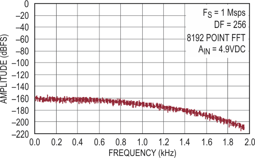
Chopper stabilized op amps such as the LTC2057 often exhibit tones at the chopping frequency and its odd harmonics. The LTC2057 utilizes circuitry to suppress these artifacts well below the offset voltage. This circuitry combined with the ADC’s own filter works to eliminate any visible tones from the op amp’s chopping frequency as shown in the noise floor plot of Figure 2. The plot of Figure 2 is an average of five data captures in an attempt to smooth out the noise floor to reveal even the smallest trace of any spurious tones.
 |
||
| Figure 2. | Noise Floor of the LTC2508-32 near FS shows no spurious tones using the circuit of Figure 1 to drive the REF pin. |
|
Conclusion
A filter circuit was demonstrated that reduces the reference output noise without compromising its accuracy or temperature coefficient while requiring only modest power consumption and cost. Applying the output of this circuit to the reference pin of the LTC2508-32, a 32-bit low noise ADC improved the SNR by up to 6.1 dB over a range of downsampling factors compared to driving the ADC directly with the reference.
