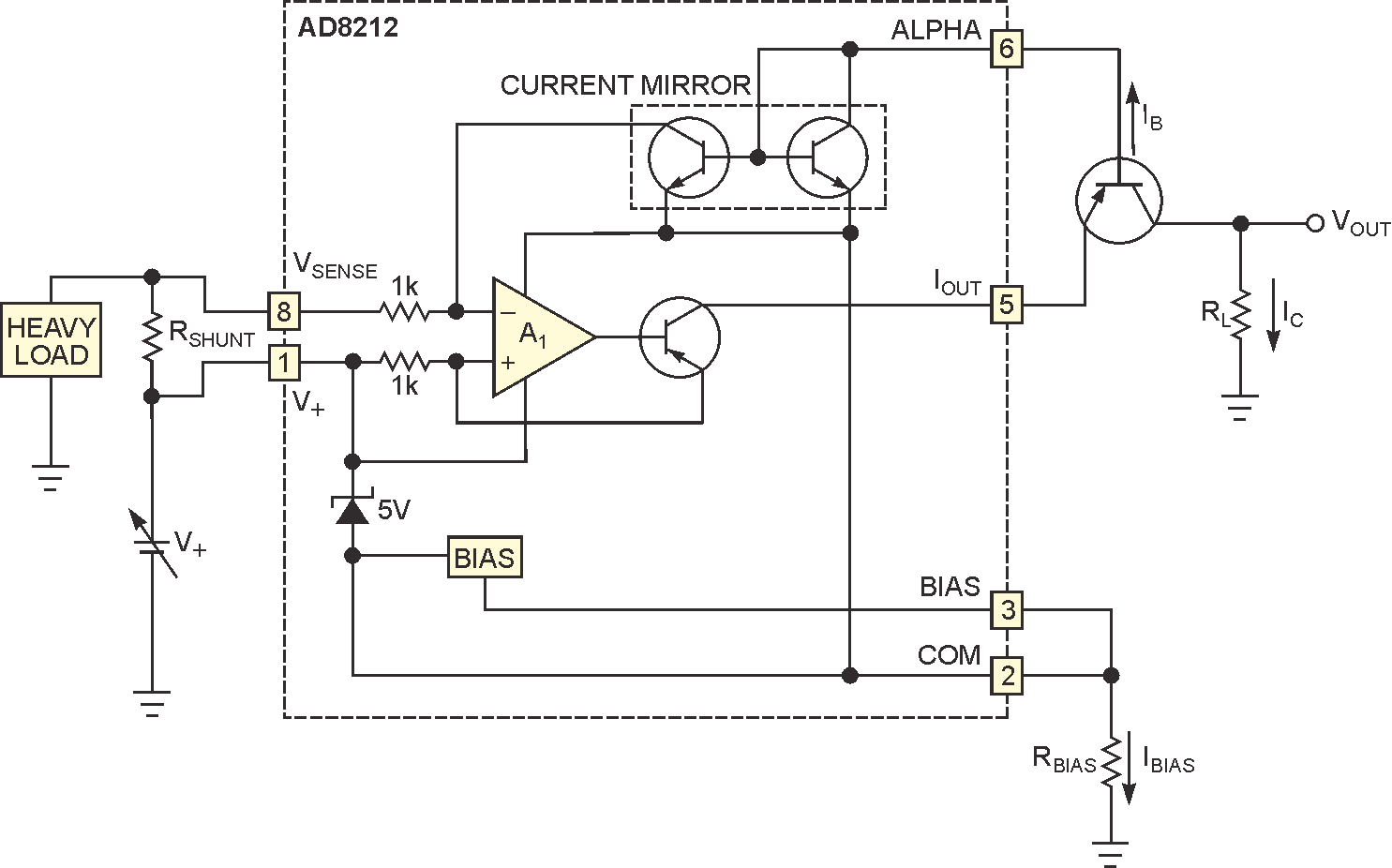
You sometimes need to measure load currents as large as 5 A in the presence of a common-mode voltage as high as 500 V. To do so, you can use Analog Devices’ AD8212 high-voltage current-shunt monitor to measure the voltage across a shunt resistor. You can use this circuit in high-current solenoid or motor-control applications. Figure 1 shows the circuit, which uses an external resistor and a PNP transistor to convert the AD8212’s output current into a ground-referenced output voltage proportional to the IC’s differential input voltage. The PNP transistor handles most of the supply voltage, extending the common-mode-voltage range to several hundred volts.
 |
||
| Figure 1. | An external PNP transistor lets you operate the circuit at high voltages. | |
An external resistor, RBIAS, safely limits the circuit voltage to a small fraction of the supply voltage. The internal bias circuit and 5 V regulator provide an output voltage that’s stable over the operating temperature range, yet it minimizes the required number of external components. Base-current compensation lets you use a low-cost PNP pass transistor, recycling its base current, IB, and mirroring it back into the signal path to maintain system precision. The common-emitter breakdown voltage of this PNP transistor becomes the operating common-mode range of the circuit.
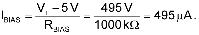
The internal regulator sets the voltage on COM to 5 V below the power-supply voltage, so the supply voltage for the measurement circuit is also 5 V. Choose a value for the bias resistor, RBIAS, to allow enough current to flow to turn on and continue the operation of the regulator. For high-voltage operation, set IBIAS at 200 μA to 1 mA. The low end ensures the turn-on of the bias circuit; the high end is limited, depending on the device you use.
With a 500 V battery and an RBIAS value of 1000 kΩ, for example,
The circuit creates a voltage on the output current approximately equal to the voltage on COM plus two times the VBE (base-to-emitter voltage), or

The external PNP transistor withstands two times the base-to-emitter voltage of more than 495 V, and all the internal transistors withstand voltages of less than 5 V, well below their breakdown capability.
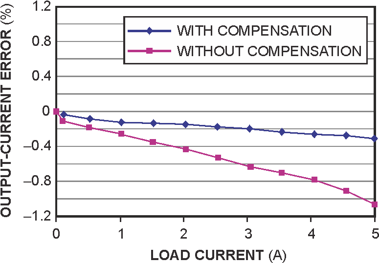
Current loss through the base of the PNP transistor reduces the output current of the AD8212 to form the collector current, IC. This reduction leads to an error in the output voltage. You can use a FET in place of the PNP transistor, eliminating the base-current error but increasing the cost. This circuit uses base-current compensation, allowing use of a low-cost PNP transistor and maintaining circuit accuracy. In this case, current-mirror transistors, the AD8212’sinternal resistors, and amplifier A1 combine to recycle the base current.
 |
||
| Figure 2. | Internal base-current compensation reduces error. | |
Figure 2 shows a plot of output-current error versus load current with and without the base-current-compensation circuit. Using the compensation circuit reduces the total error from 1 to 0.4%.You should choose the gain of the load resistor, RL, to match the input voltage range of an ADC. With a 500-mV maximum differential-input voltage, the maximum output current would be 500 μA. With a load resistance of 10 kΩ, the ADC would see a maximum output voltage of 5 V.
