Pulse-width modulation (PWM) is the best conversion method to use for digitally-controlled variable DC voltage sources requiring high accuracy and resolution. Invented 50 years ago [1, 2], the PWM approach is widely used today in switching power supplies [3] and particularly in DC calibrators [4, 5] where it is possible to achieve 26-bit resolution and 0.2 ppm linearity [6].
At the core, the PWM digital-to-analog converter (DAC) defines the DC component in a pulse train with a fixed period and a variable duty cycle. Theoretically, the DC component of such a signal is:
Generic PWM equation:
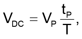 |
(1) |
where VP is pulse amplitude, tP is pulse duration, and T is the period of the signal.
To speed up the conversion process, modern DACs use a synchronous low-pass filter made of an integrator and an S/H (sample-and-hold) circuit. At the end of each period, the integrator’s voltage is stored into the S/H circuit and this is the output voltage of the whole converter.
Some converters use a feedback resistor between the output of the S/H circuit and integrator. To get a fast and accurate conversion, two time constants have to be made equal to the period of the pulse train. Reference 2 explains explicitly the requirement RF×C = T. The second requirement, RI×C = T, is not discussed, but is easy to find by applying the generic PWM equation introduced above to their equation 4.
Adjusting two time constants boils down to adjusting the integrator capacitor C or the period T of the pulse train. Both approaches face certain difficulties. The most important detail is that there are no suggestions on how to make the adjustment automatically.
This Design Idea presents a circuit and a straightforward procedure to fill the gap. Using this method requires only one adjustment. Instead of a time constant, the adjustment is made to the charging current of the integrator, which provides better resolution and linear performance.
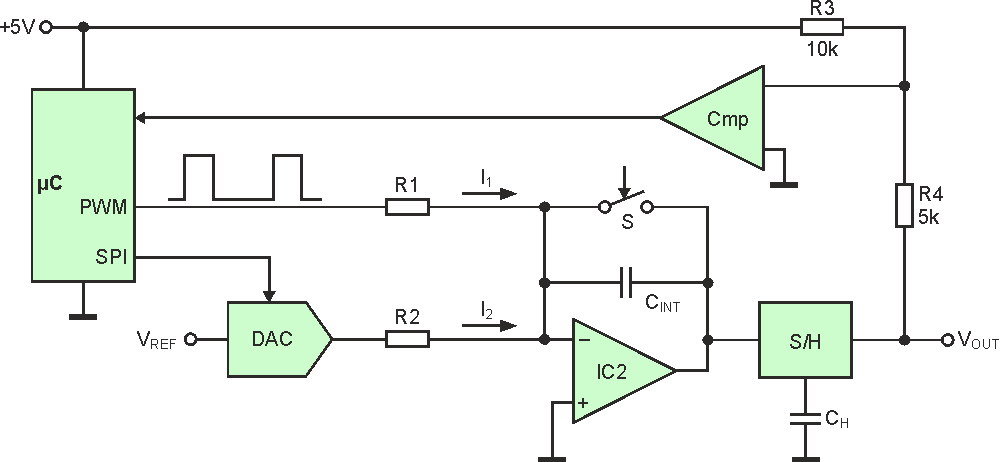
Figure 1 illustrates the concept. During the input pulse, switch S is open and an integrator capacitor is charged by two currents. The first current I1 = VP/R1 comes from the pulse train; it is 95% of the nominal current. The second current comes from an auxiliary DAC. It supplies between 0 and 10% of the nominal current, thereby providing a ±5% adjustment range for the slope of the integrator voltage. At the end of the pulse, the integrator’s voltage is stored into the S/H unit and the integrator gets discharged by closing switch S.
 |
||
| Figure 1. | An auxiliary DAC provides ±5% adjustment range for the charge current of the integrator; a comparator helps the microprocessor select the proper number for the DAC. |
|
The value of the second current is set by writing a proper number into the DAC. Each bit of the number is defined separately using the successive approximation technique. Adjustment criterion comes from Equation 1: when the duty cycle is 50%, the output voltage must be half the amplitude of the input pulses. Resistors R3 and R4 and the comparator Cmp tell the microprocessor how close the output voltage is to the required value.
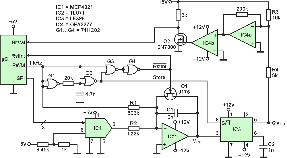
Figure 2 presents the hardware. Its operation is controlled by a timing circuit built with gates G1 through G4, which generates pulses for Q1, the reset integrator switch, and the storage switch inside the S/H unit.
 |
||
| Figure 2. | The full hardware uses a timing circuit (G1-G4) to control integrator and S/H operation, an amplifier (IC4a) to increase comparator sensitivity, and a level shifter (Q2) to interface comparator output to the microcontroller. |
|
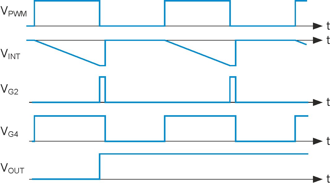
As the timing diagrams in Figure 3 show, VG4 turns high at the rising edge of the PWM signal. Reset switch Q1 opens, causing the integrator to generate a negative ramp. At the falling edge of the PWM pulse, G1 and G2 generate a 10-µs trigger pulse that makes the S/H circuit capture the integrator voltage. G3 adds VPWM and VG2 pulses to keep the reset switch open until integration and storage are complete. At the end of the storage pulse, the switch turns on. Integrator resets to zero, waiting for the next PWM pulse.
 |
||
| Figure 3. | These are timing diagrams at key points of the circuit for the first two conversion cycles. |
|
Ideally, when the pulse amplitude is 5 V and the duty cycle is 50%, the output voltage should be –2.5 V. Calibration starts with configuring the PWM system inside the microcontroller (MCU) to produce a pulse train with 1 kHz frequency and 50% duty cycle. Then the MCU sends the binary number "100000000000" to the DAC and waits for the falling edge of the RstInt pulse. When the edge comes, the microcontroller reads the comparator output. R3-R4 network and IC4 compare VOUT with the ideal value of –2.5 V. If VOUT is more positive than –2.5 V, comparator output is 0, which means the first bit in the DAC number has to change to 0; otherwise that bit keeps the preset value of 1. Then the microcontroller sends out number "x10000000000" to the DAC and adjusts the value of the second bit according to comparator reaction. The third number is "xx1000000000" and the process continues until all 12 bits of the DAC number are defined.
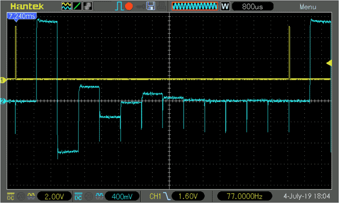
Figure 4 demonstrates the calibration process in action. The yellow trace marks the start of the procedure; it takes place at the falling edge of the RstInt pulse. The blue trace is the output signal of IC4a. It bounces on both sides of the zero voltage and gradually gets there. The value of zero means the output voltage of the S/H circuit is half the amplitude of the width-modulated pulse. The actual ratio measured by a 4.5-digit DMM was 0.49947. Using a professionally made PCB and a high-resolution multimeter will probably achieve better match.
 |
||
| Figure 4. | The successive approximation method gradually brings the output to the desired value of VP/2. |
|
After the calibration is complete, the MCU can adjust the duty cycle of the PWM signal according to customer settings. As the slope of the integrator ramp is properly set, the new voltage will appear at the output after only one period of the pulse train. Output voltage will be precisely equal to the DC component in the PWM signal as defined by theory and will have no ripples. The great thing is that you can calibrate your converter at any time and completely automatically.
Pro Tip:
To achieve the best adjustment accuracy, use a dedicated voltage reference instead of the +5 V power supply. Make sure the R3/R4 ratio is as close as possible to 2:1 and the offset voltages of IC2 and IC4 are as low as possible. R1 and R2 are metal film 1% resistors. C1 is a 2% capacitor with low dielectric absorption. Switch transistor Q1 should have small RON resistance. A higher resolution DAC can be used as well.
References
- Sugiyama T., K. Yamaguchi, Pulsewidth Modulation DC Potentiometer, IEEE Transactions on Instrumentation and Measurement, vol. IM-19, No. 4, Nov 1970, 286-290.
- Sugiyama et al., US Patent 3,636,458, Jan 1972.
- Binitha P., T. Sanish Kumar, Comparison of PWM and one-cycle control for switching converters, IJETAE, vol. 3, No. 4, Apr 2013, 332-336.
- Eccleston et al. US Patent 5,402,082, Mar 1995.
- Woodward S., DC-accurate, 32-bit DAC achieves 32-bit resolution, EDN, Oct 30, 2008, 61-62.
- Fluke, 5700A/5720A Series II Multi-Function Calibrator, Operators Manual, May 1996, page 1-8.
