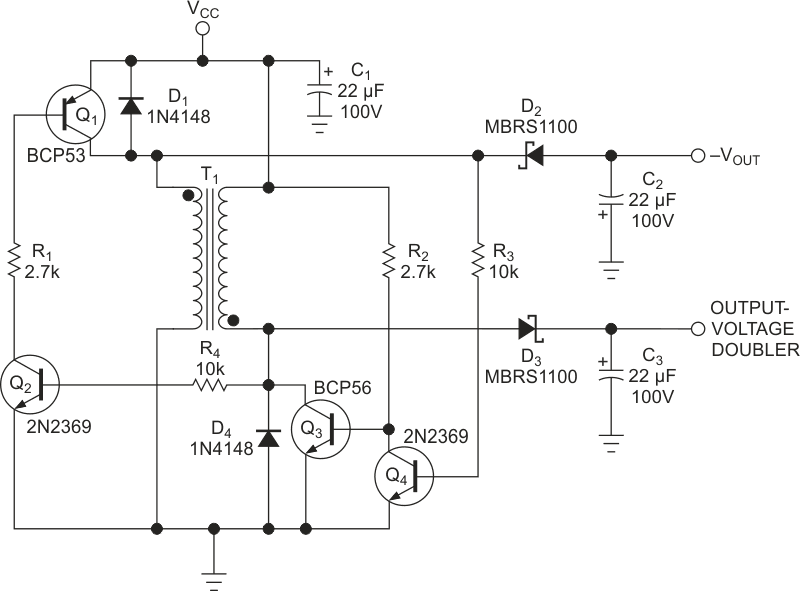
The circuit in this Design Idea uses an intrinsic property of collector voltages in one-transformer pushpull dc/dc converters: They have a swing of twice the supply voltage. When you implement these circuits with an NPN device, the collector swings from 0 V to twice the supply-rail voltage. When you use PNP devices, the collector voltage swings from VCC to an equal amplitude but negative VCC (Reference 1). In this circuit, a complementary pair of transistors, simultaneously implementing a voltage doubler and a negative- voltage source, drives the two windings of the transformer.
One of the windings of transformer T1 connects to ground, driven by PNP transistor Q1 from VCC (Figure 1). The other winding of T1 connects to VCC, and NPN transistor Q3 drives the lower end to ground. Q2 and Q4 drive Q1 and Q3, respectively. The collectors of Q3 and Q1 through resistors R4 and R3 provide cross-coupled drives to Q2 and Q4. R1 and R2 form the collector loads for Q2 and Q4. D1 and D4 prevent the reverse breakdown of Q1 and Q3. The drive configuration and the transformer’s winding polarity provide regenerative feedback and self-oscillation so that the transformer alternates between positive and negative saturation, inducing voltages to drive transistors Q1 and Q3 alternately on and off.
 |
|
| Figure 1. | Cross-coupled regeneration drives switching transistors Q1 and Q3 and the windings of the transformer. The resulting voltage swings at their collectors are rectified to twice the positive and the negative power- supply rails. |
A square wave with an amplitude twice VCC is generated at the collector of Q1, which swings nominally from VCC to the equal but negative output voltage. Simultaneously, a square wave with an amplitude twice the supply-rail voltage is generated at the collector of Q3, which swings nominally from 0 V to twice the supply-rail voltage.
D2 and C2 provide halfwave rectification and filtering of the Q1 collector waveform generating the negative voltage output. Half-wave rectification and filtering of the Q3 collector waveform using D3 and C3 generate the doubler’s output.
| Table 1. | Experimental results | ||||||||||||||||||||||||||||||||||||||||||||||||||||||||||||||||||||||
|
|||||||||||||||||||||||||||||||||||||||||||||||||||||||||||||||||||||||
T1 is 200 turns of bifilar AWG 37 enameled wire wound 1-to-1 on a ferrite toroid core. Table 1 shows the experimental results with the voltage doubler and negative-voltage-generation circuit operating over an input voltage of 5 to 30 V, demonstrating operation over a wide input voltage range and providing power at both outputs simultaneously at moderate efficiency.
Reference
- Raman, Ajoy, “Voltage doubler uses inherent features of push-pull dc/dc converter,” EDN, Aug 16, 2007, pg 72
