Introduction
In some applications it is necessary to transmit square waves across a long cable. However, long cables typically have high capacitance, which can significantly affect the signal’s wave shape. As such, the signal’s frequency and duty cycle needs to be maintained, if it is to remain free from distortion. This article discusses this phenomenon and offers a simple solution.
 |
|
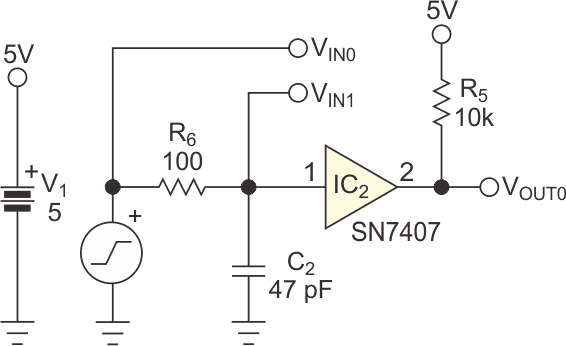
| Figure 1. | Common solution for pulse reconstruction. |
Figure 1 illustrates a common solution used to reconstruct a square wave at the end of a long cable (47 pF cable capacitance). The signal that we want to transmit is VIN0. The signal at VIN1 represents the signal at the end of the cable. You can see that this signal is very distorted by the charge and discharge of the parasitic capacitance of the cable. Furthermore, the gate (IC2) sees the rising and falling edges differently, so the reconstructed output signal will not be an accurate representation of the original digital signal.
 |
|
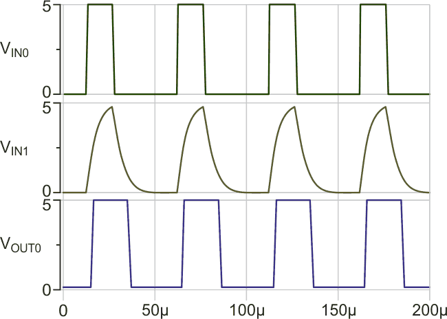
| Figure 2. | Simulation results for common pulse reconstruction. |
The circuit in Figure 2 shows that we cannot recover input pulse with a simple logic gate. We need to find a different method to detect the rising and falling edges of the digital circuits. A differentiator can be used to detect the square wave edges because the output of the RC circuit rises after the rising edge and falls after the falling edge of the square wave. Remember that the differentiator output is proportionate to the rate of change of the output signal, so it moves positively for increasing signals and negatively for decreasing signals.
 |
|
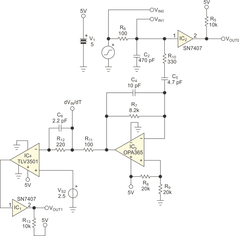
| Figure 3. | Differentiator and comparator used for pulse reconstruction. |
The design in Figure 3 uses a differentiator. Figure 3 also shows the simple gate solution (IC2) for comparison. In this example circuit, you can see how the simple gate solution does not effectively solve the problem. Note that the signal at VIN1 is from the charging and discharging of C2×R6. In this example C2 is 470 pF, or 10 times larger than the example in Figure 1. When the input pulse is high (after the rising edge), the capacitor voltage increases. The differentiator output is negative for increasing capacitor voltage (–dVIN/dT). When the input pulse is low (after the falling edge), the capacitor voltage decreases. The differentiator output is positive for increasing capacitor voltage (–dVIN/dT). Thus, by differentiating the RC signal you can reconstruct a signal that more closely resembles the original square wave. The differentiator output is followed by a comparator to create a sharp square wave output.
 |
|
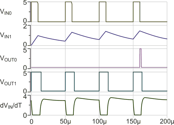
| Figure 4. | Simulation results for differentiator + comparator reconstruction. |
The simulation results for the circuit from Figure 3 are given in Figure 4. The input signal is a 20 kHz square wave with a duty cycle is 20 percent. The output of IC2 clearly does not reproduce the original signal. In fact, most of the pulses are not even detected by IC2. The differentiators output (–dVIN/dT) looks like a smoothed inversion of the original digital signal. The comparator converts the differentiator output to a sharp square wave that accurately matches the frequency and duty cycle of the original signal. Specifically, the overall error in the duty cycle for this example is approximately 10 percent.
Summary
With this circuit, we can easily implement pulse recognition after a long cable and heavy capacitance load. This method produces pulse transmission with low distortion so that the frequency and duty cycle of the original signal is preserved.
