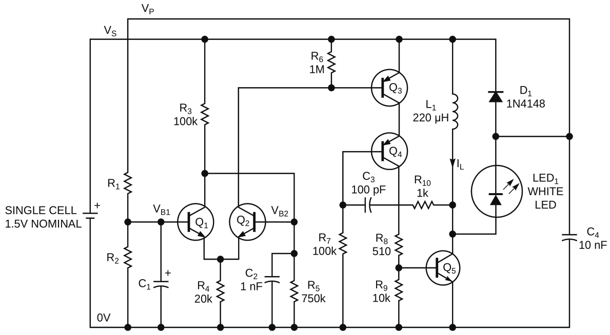
Many portable appliances and other products that must operate from a single cell are restricted to working at very low voltages. It is thus difficult to drive white LEDs that typically have a forward voltage of 3 to 5 V. The ability to flash the LED with a supply voltage as low as 1 V presents additional complications. The circuit in the Figure 1 provides a discrete approach to these problems and allows a white LED to flash at a rate set by an RC time constant. Components Q1, Q2, R3, R4, and R5 form a simple Schmitt trigger that, together with R1, R2, and C1, controls the flashing of the LED. Q4, Q5, L1, and associated components form a voltage booster that steps up the single-cell voltage, VS, to a level high enough to drive the LED. Transistor Q3 functions as a switch that gates the booster on and off at a rate determined by the Schmitt-trigger section.
 |
|
| Figure 1. | This circuit provides boosted voltage and flashes a white LED from a single cell. |
To understand how the booster section works, assume that Q3 is fully on, such that Q4’s emitter is roughly at the battery-supply voltage, VS. Q4 and R8 provide bias for Q5, which turns on and sinks current, IL, through inductor L1. The inductor current ramps up at a rate determined mainly by VS and the value of L1; during this time, LED1 and series diode D1 are reverse-biased. The current continues to ramp up until it reaches a peak value, ILPEAK. Q5 can sustain no further increase, and the voltage across the inductor at this point reverses polarity. The resulting “flyback” voltage raises LED1’s anode to a positive voltage higher than VS, sufficient to forward-bias LED1 and signal diode D1. The flyback voltage is also coupled through C3 and R10 to Q4’s base, thus causing Q4 and, hence, Q5 to turn off rapidly.
The inductor current now circulates around L1, LED1, and D1, and, as the energy stored in L1 decays, the current ramps down to zero. At this point, the inductor voltage again reverses polarity and the negative-going change is coupled through C3, rapidly turning on Q4 and, in turn, Q5. Current again begins to ramp up in L1, and the process repeats. The booster section oscillates at a rate determined by several factors. The important factors determining the rate of oscillation include the values of VS, L1, and R8; the forward-current gain of Q5; and the forward voltage of LED1. With the component values in the figure, the oscillation frequency is typically 50 to 200 kHz. On each cycle, a pulse of current with a peak value equal to ILPEAK flows through LED1 and, because this scenario occurs thousands of times every second, LED1 appears to be continuously on.
The low-frequency oscillator formed around the Schmitt trigger turns the booster section on and off at a low rate. To understand how this works, assume that Q1 is off and Q2 is on. Provided that Q2 has reasonably large forward-current gain, you can ignore the effects of its base current and say that VS and the R3-R5 voltage divider set Q2’s base voltage, VB2. With the values of R3 and R5 in Figure 1, VB2 is approximately 800 to 900 mV when VS = 1 V. This voltage produces approximately 300 to 400 mV across R4, resulting in a collector current of at least 15 µA in Q2 with R4 = 20 kΩ. Q2’s collector current provides base drive for Q3, which saturates, turning on the booster section and illuminating LED1. When LED1 is forward-biased, C4 charges to a positive voltage, VP, roughly one diode drop above VS. Timing capacitor C1 now charges via R1 at a rate determined mainly by the values of VP, R1, R2, and C1. Provided that you carefully choose the ratio of R1 to R2, Q1’s base voltage, VB1, eventually exceeds the quiescent level of VB2 (roughly equal to the Schmitt trigger's upper threshold voltage, VTU), causing Q1 to turn on and Q2 to turn off. At this point, Q3 also turns off, thereby disabling the booster section and turning off LED1.
With LED1 off, VP rapidly decays, and C1 begins to discharge at a rate determined mainly by the values of R2 and C1 and by Q1’s base current. The LED remains off until VB2 has fallen below the Schmitt trigger's lower threshold voltage, VTL, at which point Q1 turns off, Q2 turns on, and the booster section again activates, illuminating LED1. Provided that R1, R2, and C1 are large enough, LED1 can flash at a low rate. For example, if R1 and R2 have values of approximately 1 MΩ each and C1 has a value of 1 µF or greater, a rate of less than one flash per second is possible. Remember, however, that R1 and R2 form a voltage divider that sets Q1’s base voltage, VB1; therefore, R2 must be sufficiently larger than R1 to ensure that VB1 can cross the Schmitt trigger's upper threshold voltage as C1 charges. With this fact in mind, you can with some trial and error fairly easily find the optimum values of R1, R2, and C1 necessary for a given flash rate.
The value of VP significantly influences the charging and discharging of C1, and VP’s value hence varies according to the prevailing battery supply voltage, VS. However, changes in VB2, which also varies with VS, somewhat balances this dependence. Nevertheless, the flash rate and duty cycle do vary somewhat as the battery voltage falls. For example, with R1 = 2.2 MΩ, R2 = 10 MΩ, and C1 = 1 µF, the test circuit's flash rate at VS = 1.5 V is approximately 0.52 Hz with a duty cycle of 66%. With a VS of 1 V, the flash rate increases to approximately 0.75 Hz but with a lower duty cycle of 44%. The Schmitt-trigger thresholds, VTL and VTU, are typically approximately 0.7 V and 1.2 V at VS = 1.5 V, falling to approximately 0.6 V and 0.8 V when VS is 1 V.
The LED's intensity is proportional to its average forward current and is thus determined by the peak inductor current, ILPEAK, and by the duration of the current pulse through the LED. Provided that L1 is properly rated such that it does not saturate, the peak current depends largely on the maximum collector current that Q5 can sustain. For a given supply voltage, this figure depends primarily on Q5’s forward-current gain, and on the value of R8 that you can select to give optimum LED brightness at the lowest supply voltage. Experiment with different values of R8 to get the best intensity for a given LED type. Take care, however, that the peak current does not exceed the LED's maximum current rating when VS is at a maximum. The actual value of L1 is not critical, but values in the range 100 to 330 µH should provide good performance and reasonable efficiency. The transistor types in the circuit are not critical; the test circuit works well with general-purpose, small-signal devices having medium to high current gain. If possible, select low-saturation types for Q3, Q4, and Q5. C2 is not essential to circuit operation but helps to decouple any switching noise at Q2’s base.
C4 acts as a charge reservoir and ensures that R1 can charge C1 from a stable voltage source (VP) when LED1 is on. Because the charging current is likely to be low, C4 can be fairly small; a value of 10 nF should be adequate. Note that C4 must connect to the junction of D1 and LED1 as shown, rather than being charged, via a rectifying diode, from the flyback voltage at Q5’s collector. The reasons for this caveat are, first, that this approach ensures that VP is only a diode drop above VS, thereby minimizing the value of R1 necessary for a given C1 charging current. Also, and more important, this approach places the forward voltage of the LED in the path from VS through L1 and R1 to Q1’s base. Because the forward voltage of a white LED is usually at least 3 V, this connection prevents Q1 from being turned on via this route, which could otherwise cause the circuit to lock in the “off” state.
At first sight, it might appear that you can turn the booster section on and off by gating current to Q4’s base, thus obviating the need for Q3. However, under certain conditions, once you activate the booster section, the feedback to Q4’s base via C3 and R10 is sufficient to maintain oscillation without feeding any dc bias to Q4’s base. Therefore, the only reliable way to gate the booster on and off is via Q3, as shown. The test circuit starts up and operates with VS as low as 0.9 V, although the LED is dim at this voltage. The LED's intensity is good at VS = 1.5 V (equivalent to a fully charged alkaline cell) and remains acceptable with VS as low as 1 V. The circuit should find applications in toys, security devices, miniature beacons, and any other products that must provide a flashing visual indication while operating from a single cell.
