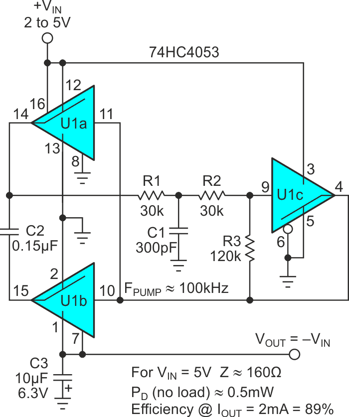
Keeping op-amp outputs “live” at and below zero volts, generating symmetrical output signals, and processing bipolar analog inputs, are all examples of design situations where a few milliamps of negative voltage rail can be a necessity. Figure 1 shows a simple inverter design based on the venerable xx4053 family of triple CMOS SPDT switches that efficiently and accurately inverts a positive voltage rail and does it for a buck.
 |
|
| Figure 1. | The generic and versatile xx4053 provides the basis for a cheap, efficient, and accurate voltage inverter. |
Here’s how it works.
U1a and U1b act in combination with C2 to form an inverting capacitor charge pump that transfers charge to filter capacitor C3. Charge transfer occurs in a cycle that begins with C2 being charged to VIN via U1a, then completes by partially discharging C2 into C3 via U1b. Pump frequency is roughly 100 kHz under control of the U1c Schmidt trigger style oscillator, so that a charge transfer occurs every 10 µs. Note the positive feedback around U1c via R3 and inverse feedback via R1, R2, and C1.
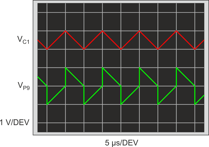
The resulting (approximate) oscillator waveforms (VC1 and U1c Vpin9) are illustrated in Figure 2.
 |
|
| Figure 2. | 100 kHz timing signals generated by the U1c Schmidt trigger oscillator. |
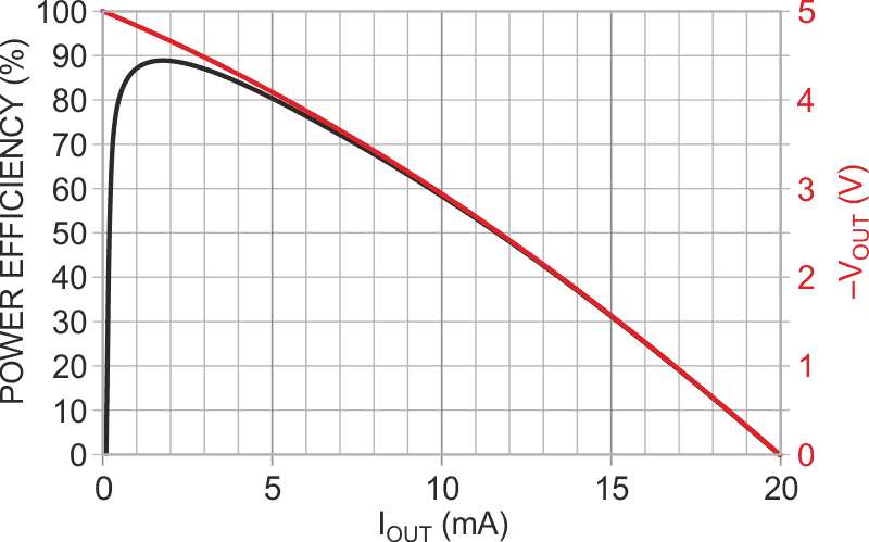
The guaranteed break-before-make switching of the xx4053 family maximizes efficiency while minimizing noise. The inherent increase of switch ON resistance with decreasing VOUT reduces shorted-output fault current to ~20 mA for VIN = 5 V. Startup at power-on requires approx 5 milliseconds.
 |
|
| Figure 3. | VOUT and power conversion efficiency versus output current for +VIN = 5 V. |
No-load power consumption is less than 500 µW and is divided more or less equally between U1 and the oscillator RC network. When VOUT is lightly loaded, it will precisely approach –1.0 × VIN. Under load, it will decline at ~160 mV/mA (Figure 3).
If operation at higher VIN inputs (up to 10 V) is required, the metal-gate CD4053B can be employed. Of course, capacitor voltage ratings would need to be correspondingly higher.
