Although adequate for undemanding applications, the circuit suffers from several drawbacks which may limit its suitability. The Darlington’s current gain (which can vary considerably from device to device and with temperature) plays a significant part in determining the circuit’s time constant, thereby making the circuit unsuitable for applications requiring precise control of the ’on’ time. Likewise, changes in supply voltage also affect the ’on’ time.
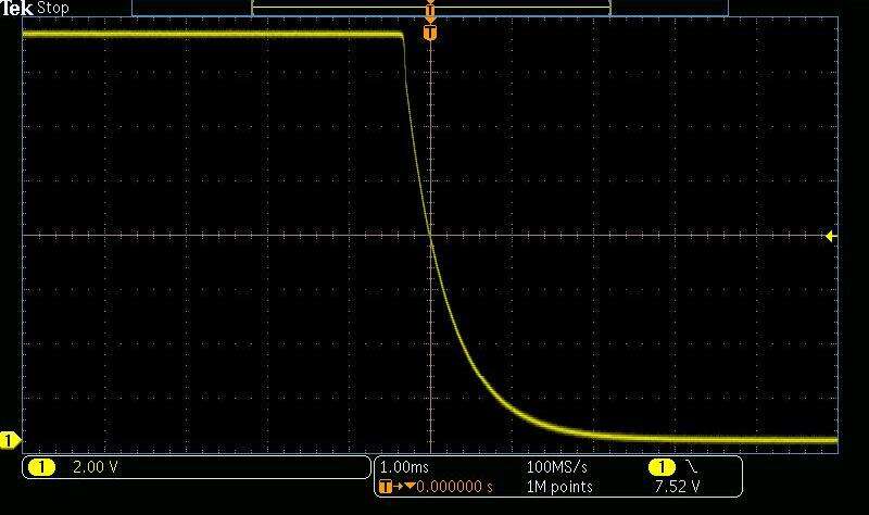
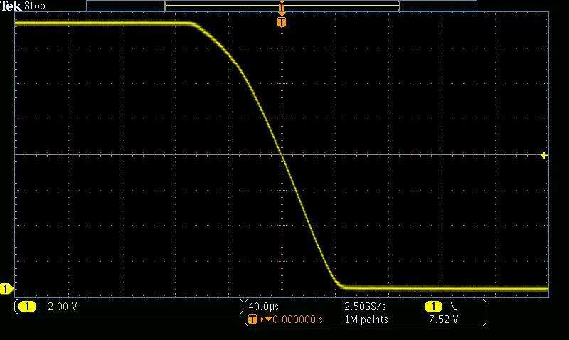
Furthermore, the fact that the Darlington’s collector current decreases gradually results in the MOSFET turning off relatively slowly. This effect can be seen in the oscillograph (Figure 4), which shows the output of a circuit powered from 15 V with a 500 Ω load using an FDS6675A MOSFET for Q2 (R4 = 1 MΩ). Note how it takes the output almost three milliseconds to transition from 15 V (the ’on’ state) to 0 V (the ’off’ state). This leisurely turn-off may be acceptable for light loads but it is not ideal behavior for MOSFETs switching large currents.
 |
|
| Figure 4. | A leisurely turn-off might be acceptable for light loads. |
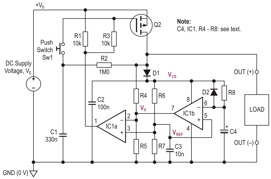
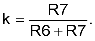
An improved version of the circuit is shown in Figure 5, where the Darlington has been replaced by a dual, open-drain/open-collector comparator (IC1), and R5 has been replaced by potential divider R4-R5. The R6-R7 divider generates a reference voltage, VREF, (a constant fraction of the comparator’s supply voltage, VCS), which provides a stable reference for both comparators.
 |
|
| Figure 5. | The improved circuit provides accurate timing, fast switching, and immunity to supply voltage changes. |
When the push switch is first pressed, Q2 turns on, energizing the load and also forward biasing D1, which provides the supply voltage, VCS, for the comparators. Now, if R4/R5 = R6/R7, the voltage VX will be slightly greater than VREF causing IC1a’s output transistor to turn on. Its output goes low (close to 0 V) thereby providing gate bias for Q2 via R3.
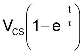
The circuit is now latched into its ’on’ state and timing capacitor C4 begins to charge via R8, and the voltage, VC, on C4 rises exponentially. At the point where VC just exceeds VREF, comparator IC1b trips and its output transistor turns on, pulling VX down to 0 V. IC1a’s output transistor now turns off and, since Q2 no longer has gate drive, the MOSFET turns off and the switch unlatches. C4 now discharges relatively quickly via the D2-R6-R7 path. As with the simpler circuit, the switch can be unlatched at any time simply by pressing the pushbutton.
Blocking diode D1 provides a dual function. It isolates R2 from the charge stored on C2 when Q2 turns off, thereby ensuring that the switch unlatches properly. Additionally, it prevents C2 (and C4) from discharging rapidly via the load when the switch turns off. This provides a brief time for the comparators to remain powered when Q2 turns off, thus ensuring that the circuit turns off in an orderly fashion. Powering the comparators from the switch output rather than from the supply voltage satisfies the fundamental requirement of all the circuits in this article, namely that (just like a mechanical switch) the power consumption in the ’off’ state is zero.
Below are the timing equations for the test circuit in Figure 5 built with IC1 = TLC393, R4 = R6 = 10 kΩ, R5 = R7 = 22 kΩ, and +VS = 15 V. Note that VCS falls out of the equations, so the ’on’ time is largely immune to variations in supply voltage.
Time delay comparator, IC1lb:
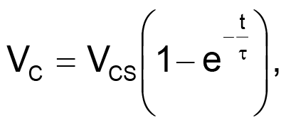
where τ = R9 × C4.
Trip-point occurs when:
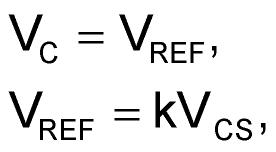
where
Equating
with kVCS gives output ‘on’ time:

or
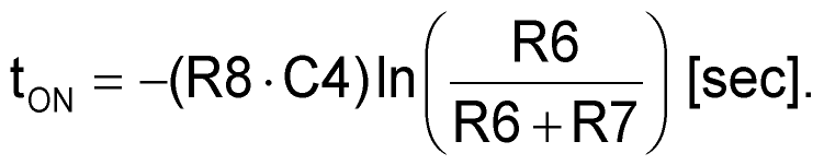
The measured and theoretical results agree well (see Table 1) except for the case where C4 = 100 µF, which produces an ’on’ time much longer than calculated. This is most likely due to internal leakage within the electrolytic capacitor used for that test (non-electrolytic types were used for the 1 µF and 10 µF tests). With suitable components, an ’on’ time well in excess of an hour could be achieved.
| Table 1. | Comparison of measured and theoretical results | ||||||||||||||||||||||||
|
|||||||||||||||||||||||||
Ignoring the drop across D1, the comparator supply voltage is roughly the same as the DC supply voltage (VCS ≈ +VS) which influences the type of comparators that can be used. The TLC393 dual micropower comparators are an ideal choice due to their miniscule power requirements and extremely low input bias current (typically 5 pA), though they are limited to a supply voltage of around 16 V. The LM393 provides an identical function and can be used with supply voltages as high as 30 V. However, the supply current is greater than that of the TLC393, and the input bias current is relatively large (typically –25 nA), which can influence C4’s charging rate. When choosing values for R4-R7, make sure that VX and VREF don’t exceed the comparators’ upper common-mode voltage limit (roughly 1.5 V below VCS for the TLC393 and LM393).
As well as providing fairly precise control over the timed output, the circuit transitions from the ’on’ to the ’off’ state much more rapidly than the simple circuit of Figure 3. The waveform shown in Figure 6 shows the output of the test circuit powered from 15 V with the same 500 Ω load and FDS6675A MOSFET as used for the simple circuit. Compared with the somewhat sluggish response in Figure 4, switching time is much improved at around 100 µs from fully ’on’ to fully ’off’.
 |
|
| Figure 6. | A modification of the circuit creates a more rapid transition from “on” to “off.” |
Choosing components
There are no special requirements for the bipolar transistors and diodes used in the preceding circuits. Provided they are rated to the maximum supply voltage, most NPN bipolars with good current gain are suitable. The P-channel MOSFET must be rated like any device used in a high-side driver circuit in terms of maximum drain-source voltage, current handling, and power dissipation. Be aware, though, that certain types of MOSFET have a maximum gate-source voltage limit much lower than the drain-source voltage rating. For example, a device like the IRFR9310 has a maximum drain-source voltage rating of –400 V, and yet the gate-source voltage is limited to just ±20 V. If your application requires a very large supply voltage, it may be necessary to fit a protective zener diode between the MOSFET’s gate and source in order to clamp the gate voltage to safe levels.
Although a push switch has been used in all the circuits, this could be replaced by, say, a reed relay (to provide a magnetically activated switch) or by some other type of momentary contacts. The only requirement is that the contacts must be electrically ’floating’ relative to the supply rails.
Finally, remember that IC1 of Figure 5 must be an open-drain or open-collector type. Also, be aware that the large impedances and sensitive nodes make the circuits susceptible to noise, which can cause false triggering and unpredictable behavior, so avoid ’messy’ construction and shield the circuits from EMI and RFI if necessary.
References
- Anthony Smith, “Latching power switch uses momentary pushbutton.”
