The key part of any electronic device is the power supply. Any instability or malfunction of the power supply part causes the device to stop working or demonstrate weird behavior. In this article, I introduced an AC/DC flyback switching power supply that converts 85 V-260 VAC to 5 VDC-2.5 A, which can be used in various applications. The 5 V selection for the output makes it friendly for linear regulators that convert 5 VDC to lower voltages.
The maximum power delivery of this power supply is around 12 W, which means it can handle 2.5 A at 5 V output. The controller chip is DK1203, which does not need any external supply, a startup resistor, or an auxiliary winding on the transformer. The ferrite core of the transformer is EE20. A potentiometer allows you to adjust the output voltage and set it exactly at 5.0 V.
I tested the board for voltage drop, current delivery, and output noise. I used Siglent SDL1020X-E DC load and Siglent SDS2102X Plus oscilloscope to perform all tests. I am confident that building this circuit enhances your knowledge regarding switching power supply design, except for using it for real applications.
Specifications
- Input voltage: 85-265 VAC
- Output voltage: 5 VDC
- Maximum output current: 2.5 A
- Maximum output current (continuous): 2 A
- Output noise (no load): 1.5 mV (rms), 4 mV(p-p)
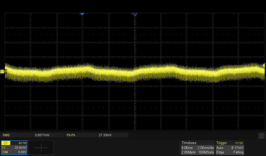
- Output noise (max load, 2 A): 3 mV (rms), 25 mV(p-p)
- Maximum voltage drop (2 A load): 50 mV
- Transformer type: EE20
Circuit analysis
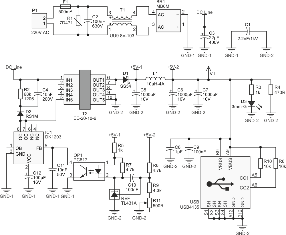
Figure 1 shows the schematic diagram of the switching power supply. As it is clear, the controller chip is DK1203.
 |
|
| Figure 1. | Schematic diagram of the flyback switching power supply. |
P1 is the input terminal for the AC input. The input voltage could be in the range of 85 V-AC to 260 V-AC and it can deliver up to 12 W of output power for this input range. F1 is a small 500 mA fuse and R1 is the 7D741 varistor to absorb high voltage transients. C2 is a 100 nF X2 rated capacitor to reduce the high-frequency noise and T1 is a common mode choke. BR1 is the Vishay MB6M bridge rectifier and C3 is a 22 µF/400 V capacitor to reduce the voltage ripple.
R2, C4, and D2 belong to the snubber circuit to dampen the switching spikes. D2 is the RS1M SMA diode. The switching controller chip is DK1203. OP1 is the PC817 optocoupler that provides an interface for the IC1 to sense the output voltage and stabilize it. REF is the TL431 shunt regulator to stabilize the output voltage and transfer any fluctuation to the optocoupler.
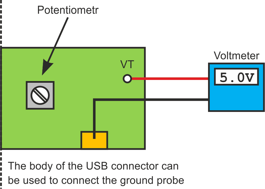
D1 is the SS54 SMC Schottky diode to rectify the output voltage. C5, C5, C7, and L1 are used to reduce the output noise. R4 is a 470R 1206 resistor that provides a preliminary load to stabilize the output voltage. D3 is a 3 mm green LED to indicate the proper operation of the power supply and output voltage. C8 and C9 reduce the high-frequency noises. VT is a test point (a single male pin header) to use a multimeter to read the output voltage, so you can use the R11 potentiometer to fix it on 5.0 V.
USB is the USB4135 USB Type-C connector to connect a USB Type-C cable to power your external devices.
PCB layout
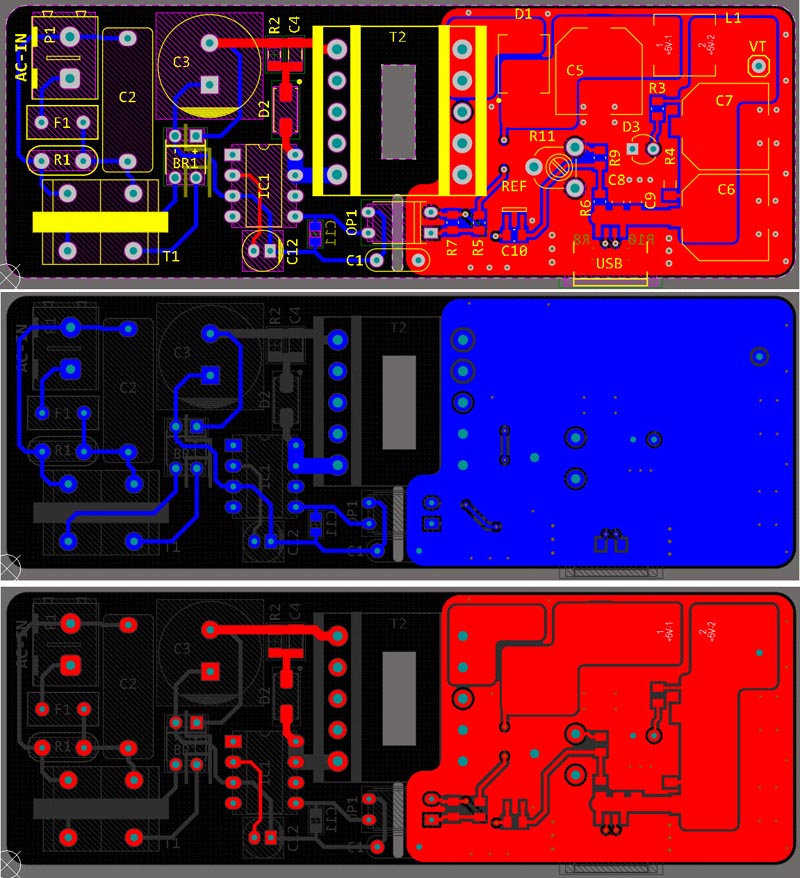
Figure 2 shows the PCB layout of the switching power supply. It’s a two-layer PCB board and I used a mixture of SMD and through-hole components.
 |
|
| Figure 2. | PCB layout of the flyback AC/DC switching power supply. |
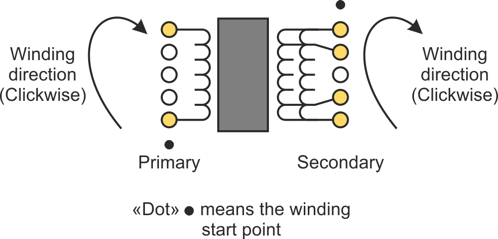
Transformer
Please follow these steps to build the transformer. First, prepare these materials:
- Core: ferrite, EE-20-10-6 (B66311G0000X187)
- Primary winding: 2.88 mH (124 turns of 0.2 mm wire)
- Gap: around 0.25 mm (mathematically)
- Secondary winding: 6 turns of 2×0.7 mm wires (two 0.7 mm wires in parallel)
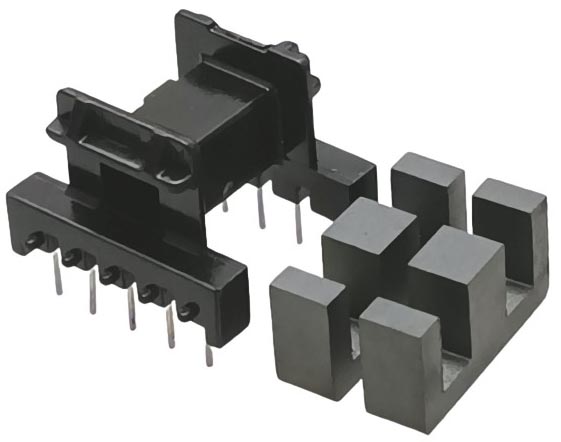
- Bobbin: 5+5, E20 horizontal (B66206B1110T001)
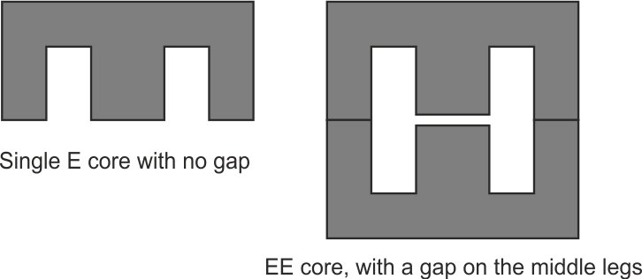
Usually, EE cores come with no gap (a gap between the two middle legs of the core). Therefore, you have to grind the middle EE legs equally to build a gap, but making such a gap accurately and winding the transformer by hand and without any error is difficult.
The easy solution is to use an LCR meter! first, wind the primary and assemble the transformer (without any gap). Then measure the inductance of the primary. Naturally, the inductance would be higher than 2.88 mH. Therefore, you have to grind the middle leg of the EE ferrite and build a gap, then assemble the transformer again and measure the inductance of the primary. As a result, simply increase the gap and continuously measure the primary inductance till it gets as close as possible to 2.88 mH.
 |
|
| Figure 3. | The 20-10-6 EE core and the non-magnetic gap of the middle legs. |
A little tolerance from 2.88 mH is fine and does not make any difference. Figure 3 shows the EE core and the gap. This is the simplest flyback transformer with one primary and one secondary winding, so you shouldn’t have any problem in this process.
 |
|
| Figure 4. | EF20 Ferrite core and 5+5 horizontal bobbin. |
Figure 4 shows the bobbin and the ferrite core. Figure 4 shows the EF20 ferrite core and bobbin and Figure 5 shows the way that you should wind the transformer.
 |
|
| Figure 5. | Transformer winding. |
Assembly and test
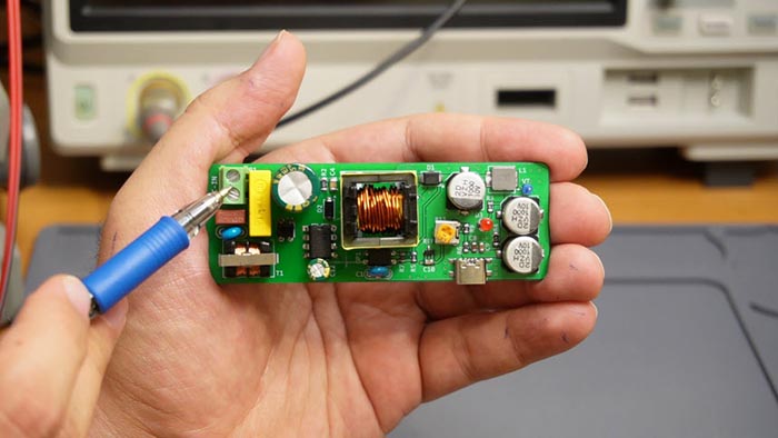
Figure 6 shows the assembled PCB board. If you have problems with soldering the components or you don’t have time to purchase and solder them yourself, you can order the board assembled.
 |
|
| Figure 6. | Assembled PCB board of the 85 V-260 VAC to 5 V flyback switching power supply. |
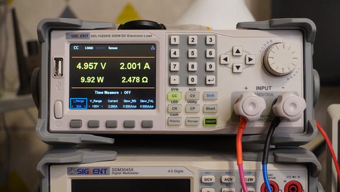
I conducted three tests for this power supply: output voltage drop, current delivery, and output noise measurement.
 |
|
| Figure 7. | The output voltage of the power supply (no load). |
Figure 7 and Figure 8 show the behavior of the power supply, first without any load and second under the maximum continuous 2 A load. As the DC load confirms, the voltage drop is just around 50 mV.
 |
|
| Figure 8. | The output voltage of the power supply (2 A load). |
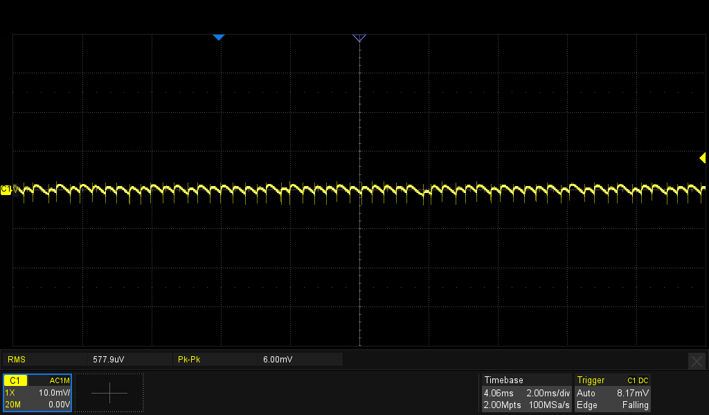
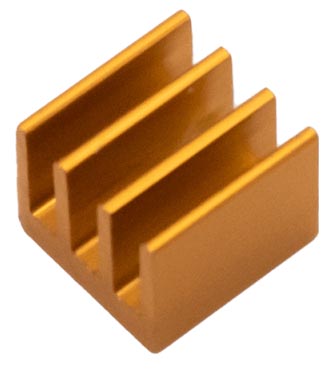
Similarly, I tested the output noise of the power supply first without any load (Figure 9) and second under the maximum continuous 2 A load (Figure 10). If you face extra heating on the output diode and inductor, mount a small heatsink on each using thermal glue. Figure 11 shows such a heatsink. VT is the testing point to connect a multimeter and adjust the output voltage to 5 V. Figure 12 shows such a connection.
 |
|
| Figure 9. | Output noise of the power supply (no load). |
 |
|
| Figure 10. | Output noise of the power supply (2 A load). |
 |
|
| Figure 11. | Suggested heatsink for D1 and L1 7×7×6 mm (if necessary). |
 |
|
| Figure 12. | Output voltage adjustment. |
