Narek Pezeshkian
Inrush current occurs in many circuits that are hot-plugged into a power supply or battery, causing the input load capacitor to experience a sudden surge of current. This surge can damage or degrade the input capacitor, generate a damaging spark upon initial contact, cause a voltage droop that can adversely affect other circuits, trip a line fuse, and generate unwanted electromagnetic interference.
Designers can use thermistors to limit inrush current. But the presence of a series resistance, the required cool-down period, or the package size may not be suitable for some circuits. Hot-swap controllers and MOSFET drivers are another choice. However, their input voltage range may be limited and they usually draw more than several hundred microamps of quiescent current, which is too much for low-power applications.
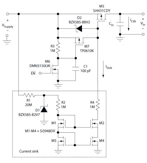 |
| 1. This inrush-current limiter uses a current sink that depletes M5's gate charge at a constant rate, resulting in a linear ramp up of VIn. Inrush current ICIN is proportional to ISink. |
The circuit in Figure 1 uses a high-side PMOS transistor to implement a simple, extremely low-power inrush current limiter with a wide input-voltage range. It presents a high-impedance load to the supply voltage (VSupply), which eliminates sparking upon initial contact. When VSupply is applied, the PMOS is slowly switched on. This eliminates a droop in VSupply and slowly ramps the input voltage (VIn) across the load’s input capacitance (CIn) to minimize the inrush current (ICIN). Due to M5’s input capacitance, its gate is initially low when VSupply is applied. But it rapidly pulls up via M7, which remains on for a period of time (adjustable by C1) longer than it takes for M5’s gate to fully charge and turn off. During this time, some amount of current passes through M5.
Designers must carefully consider the tradeoff between M5’s gate charge and RDS(ON). Yet the amount of pass-through current plus gate-charge current will be several orders of magnitude less than the inrush current without the limiter.
Simultaneously, when VSupply is applied, the cascode current mirror formed by M1-M4 begins to sink ISink amps to ground. Zener diode D1 and R1 provide a constant voltage for the current mirror, and R2 sets ISink by:
 |
(1) |
Since VDS cannot be analytically calculated from datasheet information, Spice tools or prototyping is required. Fortunately, the current mirror can use a variety of NMOS transistors.
In MOSFET data sheets, the portion of the plot of total gate charge (QG) versus gate-to-source voltage (VGS) where VGS is held constant is called the Miller Plateau. In this region, the drain-to-source voltage (VDS) changes linearly, virtually independent of the drain current.
Therefore, removing charge linearly within this region, as is done by ISink (once M7 is turned off) will ensure a linear change in VDS, causing dVIn/dt to be constant. Assuming VIn = VSupply when M5 is fully enhanced, ICIN is approximately:
 |
(2) |
where:
 |
(3) |
Here, ΔT is the VIn ramp up time, and ΔQ is the charge difference between the beginning and the end of the Miller Plateau obtained from the M5 datasheet, which can be used to calculate ΔT within a factor of 2 to 3 from the actual performance.
D2 clamps VGS(M5) = –VZener(D2), keeping it below the maximum allowed for M5. R4 isolates M2 and M4 from VSupply, reducing the total intrinsic capacitance seen by the supply voltage. Driving the gate of M6 high will rapidly deactivate M5, isolating the load from VSupply. Driving it low will once again ramp up VIn.
The choice of transistors allows a wide VSupply range. The use of logic-level transistors for M1-M7 governs VSupply(min), and a high reverse breakdown voltage (VDSS) for M2, M5, and M6 governs VSupply(max). The transistors used allow a VSupply of 3 V to 30 V. At 30 V, the maximum steady-state current consumption is less than 1.5 µA (and less than 1 µA at 20 V). The bulk of that current provides the regulated voltage for the current mirror.
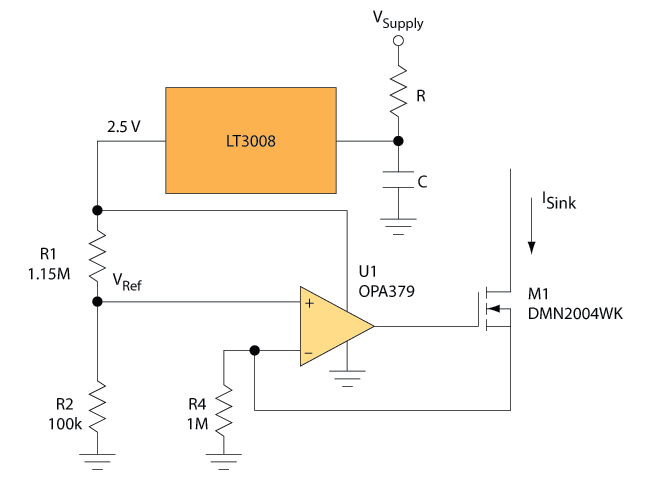 |
| 2. An alternative current sink consumes more current but relies only on VRef and R4 to set ISink. |
Figure 2 shows an alternative current sink. The rail-to-rail op amp forces VRef, which is set by R1 and R2, to appear across R4 to set ISink, in this case 200 nA. For low-voltage operations, M1 must be a logic-level NMOS. For high-voltage operations, VDSS(M1) must be greater than VSupply. A low-power linear regulator (LT3008) provides the supply voltage for the op amp. This current sink typically draws about 10 µA, but it has the advantage of relying only on VRef and R4 to set ISink.