Steven Xie, Analog Devices
Analog Dialogue
Introduction
Successive-approximation analog-to-digital converters, called SAR ADCs due to their successive-approximation register, are popular for applications requiring up to 18-bit resolution at up to 5 MSPS. Their advantages include small size, low power, no pipeline delay, and ease of use.
A host processor can access or control the ADC via a variety of serial and parallel interfaces such as SPI, I2C, and LVDS. This article discusses design techniques for reliable, integrated digital interfaces, including the digital power-supply level and sequence, I/O state during turn on, interface timing, signal quality, and errors caused by digital activity.
Digital I/O Power-Supply Level and Sequence
Most SAR ADCs provide a separate digital I/O power-supply input, VIO or VDRIVE, which determines the operating voltage and logic compatibility of the interface. This pin should be at the same voltage as the host interface (MCU, DSP, or FPGA) supply. The digital inputs should generally be between DGND − 0.3 V and VDRIVE + 0.3 V to avoid violating the absolute maximum ratings. Decoupling capacitors with short traces should be connected between the VIO pin and DGND.
ADCs that operate with multiple supplies may have well-defined power-up sequences. Application Note AN-932, Power Supply Sequencing (Ref. 1) provides a good reference for designing supplies for these ADCs. To avoid forward biasing the ESD diodes and powering up the digital core in an unknown state, turn on the I/O supply before the interface circuitry. The analog supplies are usually powered before the I/O supply, but this is not the case for all ADCs. Read and follow the data sheet to ensure the proper sequence.
Digital I/O State During Turn On
For proper initialization, some SAR ADCs require certain logic states or sequences for digital functions such as reset, standby, or power-down. After all power supplies are stable, the specified pulse or combination is applied to guarantee that the ADC starts in the intended state. For example, a high pulse on RESET, with a duration of at least 50 ns, is required to configure the AD7606 for normal operation after power up.
 |
|
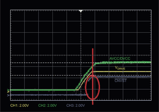
| Figure 1. | Bringing /CNVST high during power-supply ramp up could result in an unknown state. |
No digital pin should toggle until all the power supplies have been fully established. For SAR ADCs, the convert start pin, /CNVST, may be sensitive to noise. Figure 1 shows an example in which the host cPLD brings /CNVST high while AVCC, DVCC and VDRIVE are still ramping. This might put the AD7367 into an unknown state, so the host should keep /CNVST low until the supplies are all fully established.
Digital Interface Timing
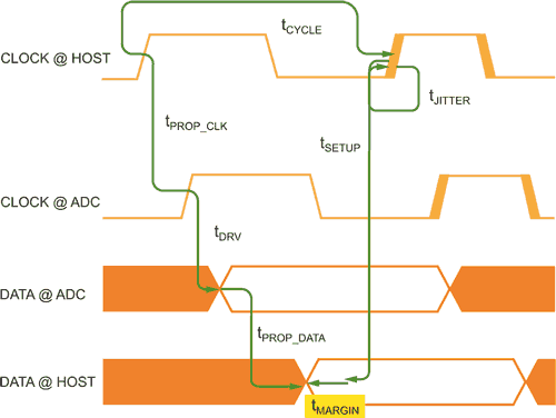
After a conversion has finished, the host can read the data via a serial or parallel interface. To read the data correctly, follow a specific timing strategy, such as which mode to use for the SPI bus. Do not violate the digital interface timing specifications, especially the setup and hold times of the ADC and the host. The maximum bit rate is determined by the whole cycle, not just the minimum specified clock period. Figure 2 and the following equations show an example of how to calculate the setup and hold timing margin. The host sends the clock to the ADC and reads the data output from the ADC.
tCYCLE = tJITTER + tSETUP + tPROP_DATA + tPROP_CLK + tDRV + tMARGIN,
where
tCYCLE: Clock period = 1/fCLOCK
tJITTER: Clock jitter
tSETUP: Host setup time
tHOLD: Host hold time
tPROP_DATA: Data propagation delay along the transmit line from ADC to host
tPROP_CLK: Clock propagation delay along the transmit line from host to ADC
tDRV: Data output valid time after clock rising/falling edge
tMARGIN: Margin time, ≥ 0 means the setup time or hold time is met; < 0 means the setup time or hold time is not met.
 |
|
| Figure 2. | Setup and hold timing margin. |
The setup margin for the host is
tMARGIN_SETUP = tCYCLE, MIN – tJITTER – tSETUP – tPROP_DATA – tPROP_CLK – tDRV, MAX.
The setup time equation defines the minimum clock period time or maximum frequency in terms of the maximum system delay terms. It must be ≥ 0 to meet the timing specifications. Increase the period (reduce the clock frequency) to handle excessive system delays. For buffers, level shifters, isolators, or other additional components on the bus, add the extra delay into tPROP_CLK and tPROP_DATA.
Similarly, the hold margin for the host is
tMARGIN_HOLD = tPROP_DATA + tPROP_CLK + tDRV – tJITTER – tHOLD.
The hold time equation defines the minimum system delay requirements to avoid logic errors due to hold violations. It has to be ≥ 0 to meet the timing specifications.
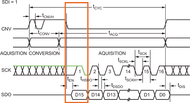
Many of ADI’s SAR ADCs with an SPI interface clock the MSB from the falling edge of CS or CNV, while the remaining data bits follow the falling edge of SCLK, as shown in Figure 3. When reading the MSB data, use ten in the equations instead of tDRV.
 |
|
| Figure 3. | SPI timing of AD7980 3-wire CS mode. |
Thus, in addition to the maximum clock rate, the maximum operating speed of the digital interface also depends on the setup time, hold time, data output valid time, propagation delay, and clock jitter.
 |
|
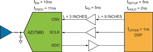
| Figure 4. | Digital interface between DSP and AD7980. |
Figure 4 shows a DSP host accessing the AD7980 in 3-wire CS mode, with VDRIVE = 3.3 V. The DSP latches the SDO signal on the falling edge of SCLK. The DSP specifies 5 ns minimum setup time and 2 ns minimum hold time. For a typical FR-4 PC board, the propagation delay is about 180 ps/in. The propagation delay of the buffer is 5 ns. The total propagation delay for CNV, SCLK and SDO is
tPROP = 180 ps/in × (9 in + 3 in) + 5 ns = 7 ns.
tJITTER = 1 ns. The host runs SCLK at 30 MHz, so tCYCLE = 33 ns.
tMARGIN_SETUP = 33 ns − 1 ns – 5 ns – 7 ns – 11 ns – 7 ns = 2 ns
tMARGIN_HOLD =11 ns + 7 ns + 7 ns – 1 ns – 2 ns = 22 ns
The setup and hold margins are both positive, so the SPI SCLK can run at 30 MHz.
Digital Signal Quality
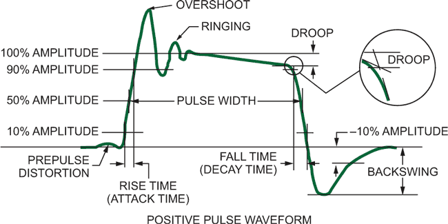
Digital signal integrity, which includes both timing and signal quality, ensures that signals: are received at specified voltage levels; do not interfere with one another; do not damage other devices; and do not pollute the electromagnetic spectrum. Signal quality is specified by many terms, as shown in Figure 5. This section will introduce overshoot, ringing, reflection, and crosstalk.
 |
|
| Figure 5. | Common specifications of signal quality. |
Reflection is a result of impedance mismatch. As a signal travels along a trace, the instantaneous impedance changes at each interface. Part of the signal will reflect back, and part will continue down the line. Reflection can produce overshoot, undershoot, ringing, and nonmonotonic clock edges at the receiver.
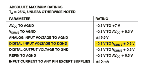
Overshoot and undershoot can damage the input protection circuitry or shorten the IC’s life span. Figure 6 shows the absolute maximum ratings of the AD7606. The digital input voltage should be between –0.3 V and VDRIVE + 0.3 V. In addition, ringing above VIL maximum or below VIH minimum may cause logic errors.
 |
|
| Figure 6. | Absolute maximum ratings of AD7606. |
To minimize reflection:
- Make the trace as short as possible
- Control the characteristic impedance of the trace
- Eliminate stubs
- Use an appropriate termination scheme
- Use solid metal with a small loop area as the return current reference plane
- Use lower drive currents and slew rates
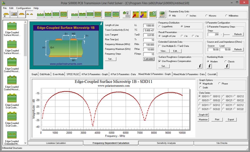
Many software tools or webs are available for calculating the characteristic impedance of a trace, such as the Polar Instruments Si9000 PCB transmission line field solver (Figure 7). These make it easy to get the characteristic impedance by selecting a transmission line model and setting parameters such as dielectric type and thickness, and trace width, thickness, and separation.
 |
|
| Figure 7. | The window of Polar Instruments’ Si9000 PCB transmission line field solver. |
IBIS is an emerging standard used to describe the analog behavior of an IC’s digital I/O. ADI provides IBIS models for SAR ADCs. Prelayout simulation checks clock distribution, chip package type, board stack-up, net topology, and termination strategies. It can also check the serial interface timing constraints to guide placement and layout. Post-simulation verifies that the design meets all guidelines and constraints, and checks for violations such as reflection, ringing, and crosstalk.
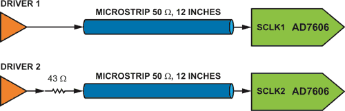
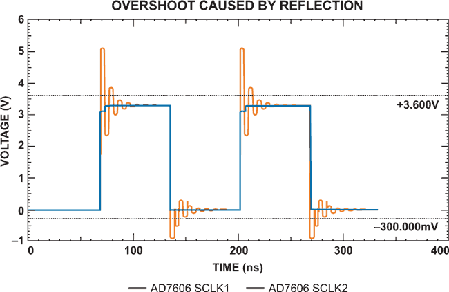
Figure 8 shows one driver connected to SCLK1 through a 12 inch microstrip line, and a second driver connected to SCLK2 through a 43 Ω resistor in series with the microstrip.
 |
|
| Figure 8. | Drive AD7606 SCLK. |
Figure 9 shows a large overshoot on SCLK1 that violates the –0.3 V to +3.6 V absolute maximum rating. The series resistor reduces the slew rate on SCLK2, keeping the signal within the specifications.
 |
|
| Figure 9. | AD7606 IBIS model simulation of overshoot. |
Crosstalk is the coupling of energy between parallel transmission lines via mutual capacitance (electric field) or mutual inductance (magnetic field). The amount of crosstalk depends on the signal’s rise time, the length of the parallel lines, and the spacing between them.
Some common practices to control the crosstalk are:
- Increase the line spacing
- Minimize parallel runs
- Keep the traces close to the reference metal planes
- Use an appropriate termination scheme
- Reduce the signal’s slew rate
Performance Degradation Caused by Digital Activity
Digital activity can degrade the SAR ADC’s performance, with the SNR decreasing due to a noisy digital ground or power supply, sampling clock jitter, and digital signal interference.
 |
|
| Figure 10. | Error voltage caused by sampling clock jitter. |
Aperture or sampling clock jitter sets the limit for SNR, especially for high-frequency input signals. System jitter comes from two sources: aperture jitter from the on-chip track-and-hold circuitry (internal jitter) and jitter on the sampling clock (external jitter). Aperture jitter is the conversion-to-conversion variation in the sampling time, and is a function of the ADC. The sampling clock jitter is usually the dominant source of error, but both sources cause varying analog input sampling times, as shown in Figure 10. Their effects are indistinguishable.
The total jitter produces an error voltage, with overall SNR of the ADC limited by
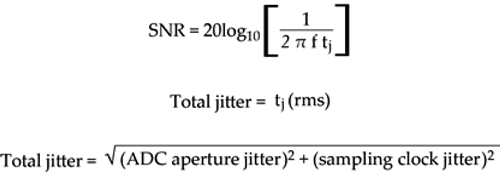
where, f is the analog input frequency and tJ is the total clock jitter.
For example, with a 10 kHz analog input and 1 ns total jitter, the SNR is limited to 84 dB.
Power supply noise caused by digital outputs switching should be isolated from the sensitive analog supplies. Separately decouple the analog and digital power supplies, paying careful attention to ground return current paths.
High-precision SAR ADCs can be sensitive to activity on the digital interface, even when the power supply is properly decoupled and isolated. Burst clocks often perform better than continuous clocks. The data sheet usually shows quiet time when the interface should not be active. Minimizing digital activity during these times – typically the sampling instant and when critical bit decisions occur – can be challenging at higher throughput rates.
Conclusion
Pay careful attention to digital activity to ensure valid conversions from SAR ADCs. Digitally induced errors may take SAR ADCs into an unknown state, cause malfunctions, or degrade performance. This article should help designers investigate root causes and provide solutions.
References
- Application Note AN-932, Power Supply Sequencing.
- Kester, Walt. “Data Converter Support Circuits.” Data Conversion Handbook, Chapter 7. Analog Devices, Inc., 2004.
- Brannon, Brad. AN-756 Application Note. Sampled Systems and the Effects of Clock Phase Noise and Jitter. Analog Devices, Inc., 2004.
- Ritchey, Lee W. Right the First Time: A Practical Handbook on High-Speed PCB and System Design, Volume 1. Speeding Edge, 2003.
- Usach, Miguel. AN-1248 Application Note. SPI Interface. Analog Devices, Inc., 2013.
- Casamayor, Mercedes. AN-715 Application Note. A First Approach to IBIS Models: What They Are and How They Are Generated. Analog Devices, Inc., 2004.
