Galvanically isolated power supplies are used in numerous applications for different reasons. In some circuits, galvanic isolation is necessary due to safety considerations. In other circuits, functional isolation is used to block any interference on signals.
A galvanically isolated power supply is typically designed with a flyback converter. These regulators have a very simple design.
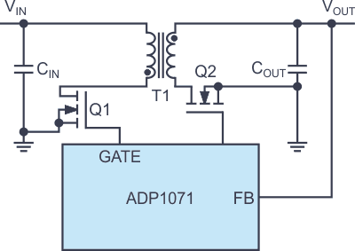
Figure 1 shows a typical design for such a regulator with an ADP1071 flyback controller. We can see that it’s a flyback converter because the dots don’t match up on the transformer. A primary-side power switch (Q1) is utilized. In addition, it requires a secondary-side rectifier circuit. This can be executed with a Schottky diode, but for higher efficiencies, an active switch (Q2 in Figure 1) is commonly used. The corresponding ADP1071 controller takes care of controlling the switches and providing the galvanic isolation for the feedback path FB.
 |
||
| Figure 1. | Shown is a typical flyback regulator (flyback converter) that handles power of up to approximately 60 W. |
|
Although flyback converters are very popular, this topology has practical limitations. The transformer T1 in Figure 1 isn’t actually used as a classic transformer. When Q1 is in the on state, no current flows through the secondary winding of T1. The energy of the primary-side current is nearly completely stored in the transformer core.
A flyback converter stores energy in the transformer, much like how a buck converter stores energy in a choke (inductor). When Q1 is in the off state, a current flow develops on the secondary side of T1. This supplies the output capacitor COUT and the output with energy. Such a concept is very easy to implement, but it has inherent limitations at higher power.
The transformer T1 is used as an energy-storage element. For this reason, the transformer can also be referred to as a coupled inductor (choke). This requires that the transformer can store the needed energy. The higher the energy class of the power supply, the larger and more expensive the transformer. In most applications, the upper limit is at approximately 60 W.
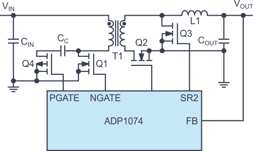
If a galvanically isolated power supply is required for higher power, a forward converter is a suitable choice (Fig. 2). Here, the transformer really is used as a classic transformer. While current flows through Q1 on the primary side, a current flow also develops on the secondary side. The transformer thus doesn’t need to provide any energy-storage capacity. In fact, however, the opposite is true. It must be ensured that the transformer is always discharged during the off-time of Q1 so that it doesn’t inadvertently reach saturation after a few cycles.
 |
||
| Figure 2. | This forward regulator (forward converter) can handle power of up to approximately 200 W. |
|
For the same power, a forward converter can use a smaller transformer than what’s required for a flyback converter. This makes the forward converter practical and sensible for use even at power levels lower than 60 W. One disadvantage is that the transformer core must be freed from unintentionally stored energy with each cycle, which is implemented by the active clamp wiring with switch Q4 and capacitor CC in Figure 2. A forward converter also usually requires an additional inductor L1 on the output side. However, through this, the output voltage may also have a lower ripple than that of a flyback converter at the same power level.
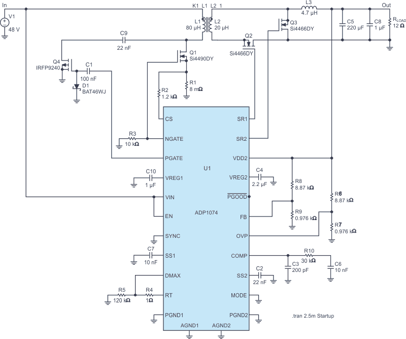
Power-management ICs such as the ADP1074 can be employed to design a forward converter. This architecture is usually used when power levels higher than approximately 60 W are required. Below 60 W, a forward converter could also be a better choice than a flyback converter based on circuit complexity and achievable efficiencies. To simplify the decision on which topology to use, simulation with the free circuit simulator LTspice is recommended. Figure 3 shows the simulation schematic of an ADP1074 forward-converter circuit in the LTspice simulation environment.
 |
||
| Figure 3. | Example of a circuit with an ADP1074 simulated in LTspice. | |
