Introduction
Wide bandgap power semiconductor devices like Silicon Carbide (SiC) MOSFETs are enjoying growing popularity in many modern power electronic applications like E-mobility and renewable energy. Their extremely fast switching speed capability helps to increase efficiency and reduce the overall size and cost of the system. However, fast switching together with high operating voltages and increasing switching frequencies presents important challenges to the gate driver system. Rugged galvanic isolation, compliance with safety standards, control signal noise immunity and EMI performance are just some of the most important aspects to consider. An optimal design of the isolated auxiliary supply providing the voltage and current levels to drive the SiC/GaN device is critical to help the full gate driver system meet the many requirements set by state-of-the-art applications.
Overview and requirements for gate control of HV SiC/GaN FET devices
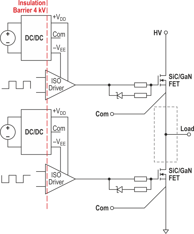
In applications using SiC/GaN high-voltage semiconductor devices under hard-switching operation, galvanic isolation is a common requirement for safety and functional reasons, and depending on the application, a basic or a reinforced insulation will be required. The operating voltage, insulation material, pollution degree and the applicable regulatory standards set the minimum creepage and clearance distances as well as the dielectric isolation voltage requirement affecting the components placed across the isolation barrier. The high-speed isolated gate driver IC (e.g. TI UCC21520) and the transformer in the isolated auxiliary power supply (DC/DC Block in figure 1) both ‘bridge’ this isolation barrier, thus having to meet stringent safety and functional requirements.
 |
|
| Figure 1: | Overview of a HV half-bridge control of the High-side & Low-side SiC-MOSFET. |
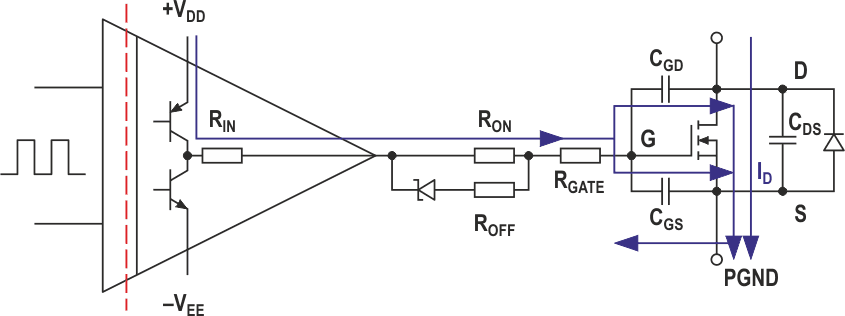
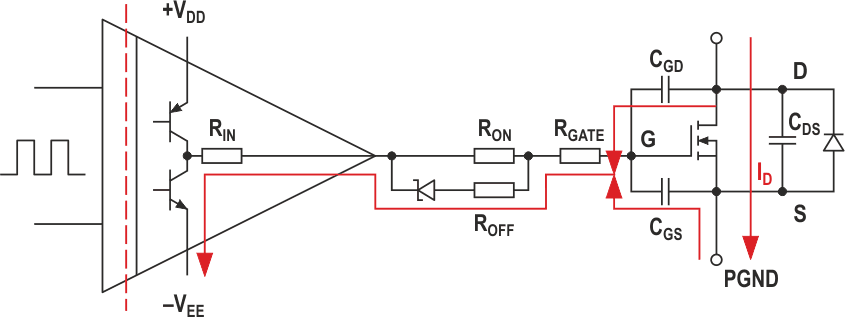
The latest SiC MOSFETs require gate-source voltages between +15 V and +20 V to fully turn on and between 0 V and –5 V to reliably turn off. For the gate of a gallium nitride FET (GaN 650 V) usually only +5 V and 0 V are required. In some cases, a small negative voltage is also used to turn off the GaN FET. Please note that these values vary depending on manufacturer. In figure 1, a half-bridge configuration is shown, and several of these stages are typically required in an inverter circuit to drive AC-motors in the kW range. Each SiC/GaN FET would require an independent gate driver stage with its own isolated auxiliary supply. This not only enables individual control of each SiC/GaN device, but also helps to keep the gate current loop small and local to the device, minimizing the adverse effects of parasitic loop inductance and ground bounce caused by the very high ΔI/Δt generated during the switching transition (figure 2 and figure 3).
 |
|
| Figure 2: | High ΔI/Δt current paths on turn-ON of SiC/GaN FET. |
 |
|
| Figure 3: | High ΔI/Δt current paths on turn-OFF of SiC/GaN FET. |
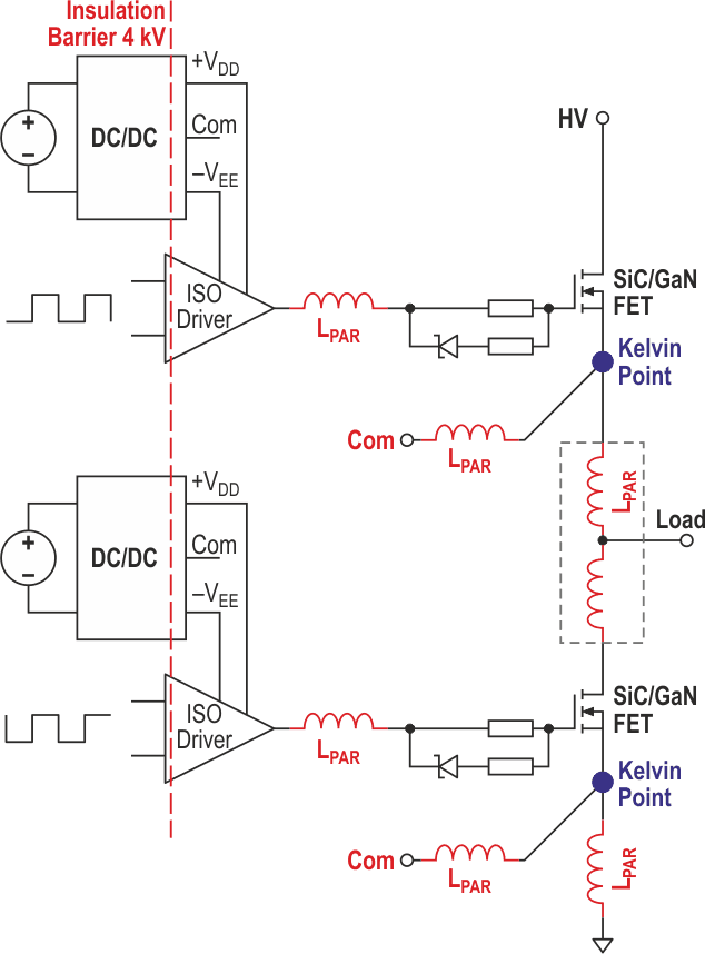
If ignored, this may lead to uncontrolled turn-on/off of the MOSFET and thermal issues. Some SiC MOSFETs are designed with an additional low impedance Kelvin source connection for a gate current return path (figure 4).
 |
|
| Figure 4: | Kelvin connections and critical parasitic inductances in a half-bridge configuration. |
This connection does not carry the high switching current and therefore has a lower interference potential due to lower parasitic inductance than the source connection, which significantly improves gate driving (e.g. Infineon IMZ120R045M1 1200 V / 52 A).
Regarding the auxiliary supply, its output capacitors (with minimal ESL and ESR) should be placed very close to the gate driver IC and SiC/GaN device to minimize the gate current loop and with it its parasitic inductance in order to reduce the associated parasitic effects (i.e. ringing).
Requirements of the isolated gate driver power supply for SiC-MOSFETS
There is currently a large selection of compact, isolated 1 – 2 W DC/DC converters available on the market. For a SiC-MOSFET like the Infineon IMZ120R045M1 1200 V/ 52 A, up to 1 W power requirement per device can be estimated (see example calculation (1)). However, an application with over 5 kW load power would require the use of either a SiC-MOSFET module (e.g. ROHM BSM600D12P3G001 1200 V/ 600 A) or alternatively several discrete SiC-MOSFETs in parallel (current sharing). In a module solution, several semiconductor dies are paralleled to form the final SiC-MOSFET. This technique reduces the effective RDS(ON) but results in a higher "Total Gate Charge", requiring more driver power from the auxiliary supply (example calculation (2)). Above 2 W of power, there is only a very limited selection of off-the-shelf isolated DC-DC converter modules, which despite their convenience, they often come at a premium cost while being larger than discrete solutions and with efficiencies lining under 80%.
PGATE = PDRV + (QGATE·FSW·ΔVGATE)
PGATE – total power required to drive the SiC device gate;
PDRV – power loss in the gate driver section (approx. 0.3 W);
QGATE – total Gate Charge value (from datasheet);
FSW – maximum switching frequency;
ΔVGATE – maximum voltage swing at the gate from –VEE to +VDD (e.g. –4 V to +15 V = 19 V);
Example calculation (1) with Infineon IMZ120R045M1 1200 V / 52 A:
PGATE = 0.3 W + (62 nC·100 kHz·19 V) = 0.42 W.
Example calculation (2) with ROHM BSM600D12P3G001 1200 V / 600 A:
PGATE = 0.3 W + (1900 nC·100 kHz·19 V) = 3.91 W.
The currently available SiC MOSFET modules can feature a total gate charge from as little as a few hundred nC up to 3000 nC. The higher their blocking voltage and rated power, the higher their gate capacitance. With an increase in the switching frequency or load power (requiring more SiC devices connected in parallel with the corresponding increase in total gate charge) 6 - 10 W of driver system power can be expected for the most demanding current and future applications.
Efficiency, size and especially the parasitic coupling capacitance are all important parameters in high-performance SiC-based systems. With increasing switching speed and the resulting very steep switching slopes, more harmonic energy is capacitively coupled between the converter output stage/gate driver (high-voltage side) and the low-voltage control side.
The parasitic capacitance (CP) between primary and secondary sides in the gate driver auxiliary supply is mainly set by the interwinding capacitance of the DC/DC power transformer device. With latest SiC-MOSFETs switching at ΔU/Δt slew-rates of 100 kV/µs, 10 pF parasitic capacitance would cause a peak displacement current of 1 A across the isolation barrier. A high displacement current degrades the insulation barrier in the long run, interferes with the control signals and leads to common mode currents, which are a typical cause of EMI problems.
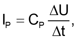
IP – electrical displacement current,
CP – parasitic coupling capacitance.
It is generally recommended to keep CP in the auxiliary supply below 10 pF.
However, consider that the maximum capacitance tolerated in any application depends on the switching speed and CMTI (Common-mode Transient Immunity) capability of the gate driver IC used.
