By Darwin Tolentino
The controller area network (CAN) serial-bus topology allows devices and microcontrollers to communicate with each other without the use of a host computer. Featuring arbitration-free transmission, it places a controller and a host processor at each device node, eliminating the more complex wiring harness that would be necessary to interconnect devices with a host computer.
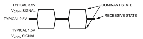
By using the signals on CANH and CANL wires, the CAN bus has two states: recessive and dominant (Figure 1). The bus is in the dominant state if the differential voltage is greater than 0.9 V and in the recessive state if it is less than 0.5 V. CAN transceivers, such as the ADM3051 , interface the CAN controller to the physical layer bus.
 |
|
| Figure 1. | CAN bus signals and states. |
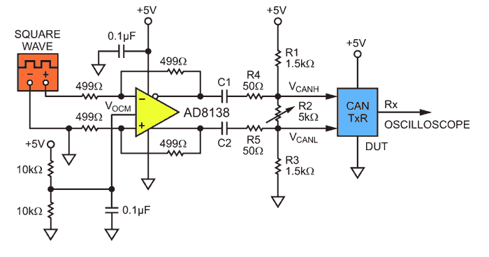
A CAN transceiver can be characterized using automated test equipment (ATE) or dc signals on a bench. The circuit shown in Figure 2 uses a square wave signal from a function generator to provide adjustable CAN signals to a transceiver. The AD8138 high speed differential amplifier was chosen for its wide bandwidth and low distortion. A dc level shifter at the output enables the differential level of the output signals to be adjusted while maintaining their peak-to-peak levels. The amplitude and frequency are adjusted via the signal generator.
 |
|
| Figure 2. | AD8138 drives CAN transceiver. |
Operating from a single 5-V supply, the circuit is configured as a unity-gain single-ended-to-differential amplifier with common mode set at midsupply. R1, R2, and R3 form the dc biasing circuit that scales the output signals to CAN levels. By keeping R4 and R5 small compared to R2, the potentiometer conveniently adjusts the difference between the two output signals without significantly affecting their individual amplitudes, providing a CAN signal with a variable common-mode level to the DUT. Because R1 and R3 are equal, the ac common mode of the outputs is also unaffected when adjusting R2. Together with R2, R4 and R5 form part of the voltage divider at the output of the AD8138 amplifier. The smallest possible values are chosen for R4 and R5 to minimize the attenuation at the output and the effect of adjusting R2 on the peak-to-peak level of each output. If R2 is shorted, R4 and R5 will also provide the minimum load to protect the amplifier’s output. Capacitors C1 and C2 isolate the dc bias from the amplifier’s output common mode. These capacitors also form a high-pass filter with the resistor bias network; its cutoff frequency is:
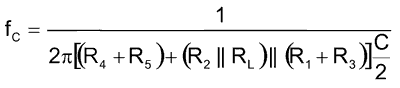
where C = C1 = C2, and RL is the load or DUT input resistance, typically around 20 kΩ to 30 kΩ.
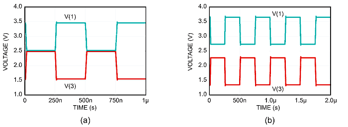
To avoid distorting the square wave output signals, C1 and C2 should be chosen as large as possible so that the input signal frequency is 10 times the worst-case cutoff frequency, where R2||RL is at minimum. For example, to achieve VCANH and VCANL signals with the levels shown in Figure 3(a), R2 must be a minimum of 700 Ω, assuming no output (DUT) loading effect. A 0.1 µF or 1 µF coupling capacitor can accommodate a 1-MHz signal. Figure 3(b) demonstrates how R2 adjusts the differential output levels.
 |
|
| Figure 3. | VCANH and VCANL outputs. |
Using these output signals as VCANH and VCANL inputs to a transceiver enables bench scope measurements to characterize receiver parameters such as propagation delay, rise time, and thresholds on desired frequencies.