Introduction
The I2C Bus Sniffer allows for non-intrusive monitoring of an I2C bus. All data, including device addresses, ACK/NAK, START and STOP conditions, are reported in textual form to a serial terminal.
A familiar theme in open-source projects is “a need to scratch an itch.” In my case, the itch was a need to know exactly what was happening on an I2C bus on a certain system at work. Commercial products are available, but the immediate cost (versus engineering time, which is a cost spread over time) was too high to justify it. In the end, I hooked up a logic analyzer, captured the SCL and SDA lines, and the deciphered the protocol by hand. That fixed the immediate problem, but I didn’ t want to do that again, and I resolved to create my own I2C bus monitor in my spare time. The I2C bus was developed by Philips in the 1980’ s. It is a serial bus, consisting of a clock and data line. The protocol specifies START and STOP conditions, the data format (8 bits, MSB first), and and ACK/NAK bit. Refer to [1] for the complete specification. Aside from minimum widths, the clock pulses do not have to be of the same width, which makes the bus quite flexible for implementation on even the smallest microcontrollers.
Software and Hardware Co-Design
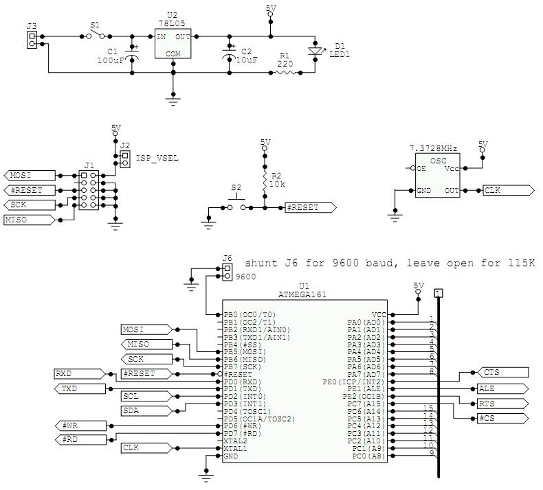
The I2C bus can run at [almost] any speed, but is commonly seen at 100 KHz and 400 KHz. A 3.4 MHz enhancement shows up in a few places. Since the systems I was working on involved a 100 KHz bus, I decided that an 8MHz AVR would suffice.
Most serial ports on PC’ s can run as fast as 115,200 baud. If the data is transmitted as ASCII, each byte on the I2C bus will take two bytes on the serial port. This 2x disparity will quickly cause problems in buffering, and so I chose to add 32KB of external RAM, to be used as a circular buffer. The bus monitor routine appends data at the tail, and the serial port routine pops data off the head. Simple program logic wraps the pointers back to the start of external RAM when they go off the end of 32KB.
The basic building block is therefore an ATMEGA161 (I know, I should upgrade to a 162, but I had the 161 laying around already) with a latch (74F573) and 32KB of SRAM. I happened to have several old cache chips (20ns 32KB SRAM’ s) from a 486 system laying around, and they work nicely. I needed both the external RAM interface, and I needed “either edge” sensitivity on at least one interrupt line. DIP package availability was the final deciding factor.
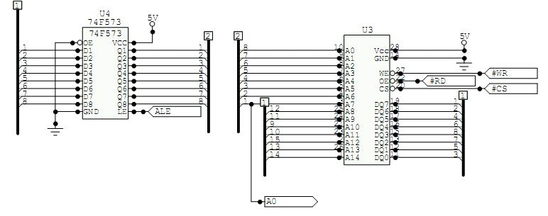
I wasn’ t entirely confident in my external SRAM (they were salvaged from a dead system), and so I wrote a memory test to validate the chips. On the hardware design, I took the easy way out on the SRAM and used A15 for a chip select, thereby basing the RAM at address 0. This is fine, except that the AVR maps internal RAM to address 0, and the external RAM isn’ t selected until you access past the end of internal RAM. This made it basically impossible to do a “walking bits” test on the address bus, and so I fell back on another trick in my bag o’ tricks: the pseudo-random pattern.
I used a linear-feedback shift register, in a Galois configuration, to test the memory. LFSR’ s are provably weak in cryptography (where they are often misused), but I’ m just looking for a pattern that won’ t repeat within my constraints, and so this will suffice. The idea is to write different values to each successive memory location, thereby uncovering failures such as data or address bits shorted to each other, ground or Vcc, or even something as simple as a memory chip entirely missing. The memory test code, while interesting in its own right, is here merely a means to an end, and will not be discussed further.
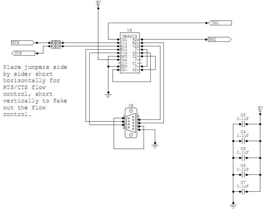
On the hardware side, I had initially planned what is now called “the grandiose vision,” which was a small, self-contained unit that would attach to any system I needed to monitor. Certain options would be available for dropping down to 9600 baud (where the 32KB of external buffer would be even more important) when I was connected to a [very] dumb terminal, as well as utilizing RTS/CTS flow control. Even better, I planned to use opto-isolators to further protect the Unit Under Test from the bus monitor, and vice-versa.
This is the “subset” version of the hardware. If I had an STK501, this wouldn’ t have been necessary, but I don’ t have an STK501, and so I needed a way to hook up the external SRAM. With the subset hardware on the STK500, I was able to focus on the software instead of worrying about the hardware.
All of the heavy work is done inside ISR’ s. An I2C bus START or STOP condition consists of the SDA signal changing when SCL is high, so I wrote an ISR to be called on either edge of SDA. On entry, it tests SCL. If it is low, the ISR exits immediately. Otherwise, the “new” level of SDA determines if we have just seen a START or STOP condition. The condition is recorded in RAM (“S” for START, “P” for STOP, as per the common usage I have seen in other documents), bit counters are reset, and we exit. The interrupt for SCL (to capture data bits) is enabled after seeing a START condition, and disabled after seeing a STOP condition.
To capture data bits, I only need the rising edge of SCL. Each interrupt, I sample the SDA pin to see if I have a 1 or 0 bit. The bit is rotated into a register designated for capturing the data, and the bit count is incremented. Once I have 8 bits, I convert to ASCII and store in RAM. The next bit will be an ACK or NAK, which I capture and store in RAM as an “A” or “N.” Storing data in RAM is done in a subroutine so I can check to make sure we haven’ t walked off the end of 32KB. If so, we reset to the beginning of external RAM and continue.
Once completed, the “subset” hardware on an STK500 was perched atop a CompactPCI chassis. I powered on the STK500, observed the memory test results (pass), and then powered on the unit under test. Here is a sample of the output from the bus sniffer, as it monitors the aforementioned unit under test:
S C0 A 73 A E2 A 05 A 00 A 00 A P
S C0 A 00 A 7F A 5F A 55 A 00 A P
S C0 A 02 A 1F A 07 A 99 A A0 A P
S C0 A 5C A 00 A 00 A 00 A D8 A P
S C0 A 78 A 00 A 80 A 10 A CC A P
S C0 A 7B A E0 A 05 A 00 A 00 A P
S A0 A 00 A S A1 A 31 A 31 A 31 A 31 A 31 A 31 A 31 A 31 N P
S C0 A 21 A 00 A 00 A 05 A 58 A P
S C0 A 21 A S C1 A 00 A 00 A 00 A 80 N P
The unit writes to registers on the device at address 0xC0, reads data from the EEPROM at address 0xA0 (note the Repeated Start condition, followed by address 0xA1), writes again to 0xC0, and then reads (again, a Repeated Start) from 0xC1. After I got all the kinks out of the software, I went back to my full PCB and found a few problems. The worst was the opto-isolators for the SDA and SCL signals. Depending on the values of the resistors, I wound up either pulling the SDA and SCL signals too low on the unit under test (thereby hanging the bus), or the signal passing through the opto-isolator was too weak to register as a “high” on the AVR. I’ ll have to revisit the isolator design at some point in the future. Until then, I can simply jumper across the resistor
posts and forego the opto-isolation.
The AVR must process several instructions for each bit on the I2C bus. This limits the maximum bus speed that can be reliably monitored to 100 KHz. Anything beyond that will require extra logic to capture the serial stream and present it to the microcontroller for further processing. This could be an interesting future project for an FPSLIC.