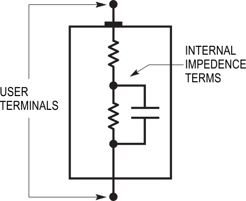
It is often desirable to determine a battery’s internal resistance to evaluate its condition or suitability for an application. Accurate battery resistance determination is complicated by inherent capacitive terms which corrupt results taken with AC-based milliohmmeters operating in the kHz range. Figure 1, a very simplistic battery model, shows a resistive divider with a partial shunt capacitive term. This capacitive term introduces error in AC-based measurement. Additionally, the battery’s unloaded internal resistance may significantly differ from its loaded value. As such, a realistic determination of internal resistance must be made under loaded conditions at or near DC.
 |
|
| Figure 1. | Simplistic model shows battery impedance terms including resistive and capacitive elements. Capacitive component corrupts AC-based measurement attempts to determine internal DC resistance. More realistic results occur if battery voltage drop is measured under known load. |
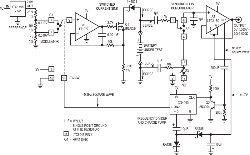
Figure 2’s circuit meets these requirements, permitting accurate internal resistance determination of batteries up to 13 V over a range of 0.001 Ω to 1.000 Ω. A1, Q1 and associated components form a closed loop current sink which loads the battery via Q1’s drain. The 1N5821 provides reverse battery protection. The voltage across the 0.1 Ω resistor, and hence the battery load, is determined by A1’s “+” input voltage. This potential is alternately switched, via S1, between 0.110 V and 0.010 V derived from the 2.5 V reference driven resistor string. S1’s 0.5 Hz square wave switching drive comes from the CD4040 frequency divider. The result of this action is a 100 mA biased 1 A 0.5 Hz square wave load applied to the battery. The battery’s internal resistance causes a 0.5 Hz amplitude modulated square wave to appear at the Kelvin-sensed S2-S3-A2 synchronous demodulator. The demodulator DC output is buffered by chopper stabilized A2 which provides the circuit output. A2’s internal 1 kHz clock, level shifted by Q2, drives the CD4040 frequency divider. One divider output supplies the 0.5 Hz square wave; a second 500 Hz output activates a charge pump, providing a –7 V potential to A2. This arrangement allows A2 output swing to zero volts.
 |
|
| Figure 2. | Battery internal resistance is determined by repetitively stepping calibrated discharge current and reading resultant voltage drop. S1-based modulator, clocked from frequency divider, combines with A1-Q1 switched current sink to generate stepped, 1 ampere battery discharge cycles. S2-S3-A2 synchronous demodulator extracts modulated voltage drop information, provides DC output calibrated in ohms. |
The circuit pulls 230 μA from its 9 V battery power supply, permitting about 3000 hours battery life. Other specifications include operation down to 4 V with less than 1 mV (0.001 Ω) output variation, 3% accuracy and battery-under-test range of 0.9 V to 13 V. Finally, note that battery discharge current and repetition rate are easily varied from the values given, permitting observation of battery resistance under a variety of conditions.
