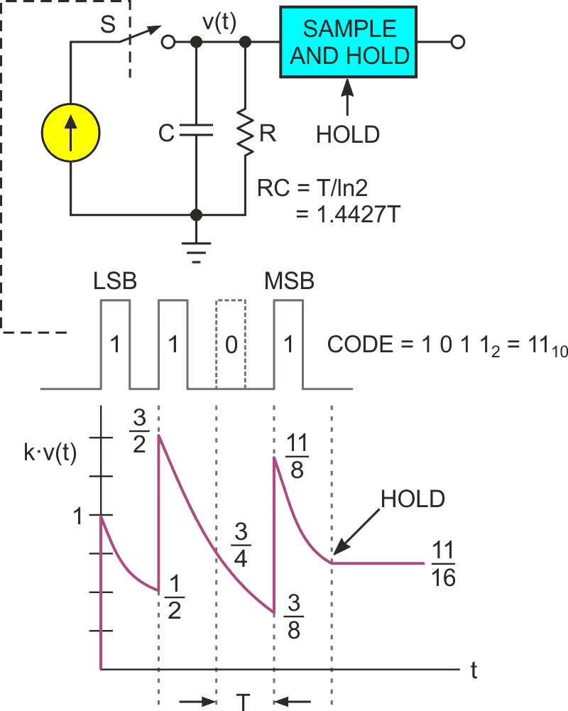
If you need to quickly and inexpensively convert a binary number into a proportional analog voltage, one cool (and easily remoted) way to do it is:
- 1. Serialize the number into a bit stream with the LSB output first,
- 2. input the resulting stream into an RC time constant with
- 3. RC = T/ln(2), where T = the inter-bit interval, and
- 4. capture the final integrated voltage at the end of bit string input with a S&H.
This method is conceptualized as the Shannon decoder DAC (SDD) in Figure 1 [1].
 |
|
| Figure 1 | The Shannon decoder DAC (SDD) concept. |
Applying the SDD concept to implementation of a DAC (or multiple DACs) benefits from some useful facts.
- Serializing and outputting binary numbers with LSB first is exactly what the standard universal asynchronous receiver/transmitter function (UART) does, and
- UARTs are widely and inexpensively available, both as USB-driven external RS232 peripherals for PCs (typically using the popular FTDI or similar chipsets and available fully cabled and connectorized for less than $10) and as internal peripherals in popular microcontroller chips (the TM4C123x contains eight!).
 |
|
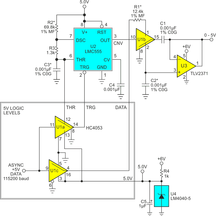
| Figure 2 | The SDD with 5V asynchronous serial data, similar to a µC UART output. |
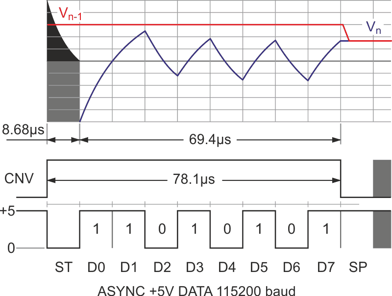
Figure 2 illustrates an SDD for 5-volt asynchronous serial data of the sort a µC UART might output, and Figure 3 is its timing diagram. Here’s how it works.
 |
|
| Figure 3 | The SDD conversion cycle timing for 5 V logic levels. |
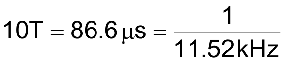
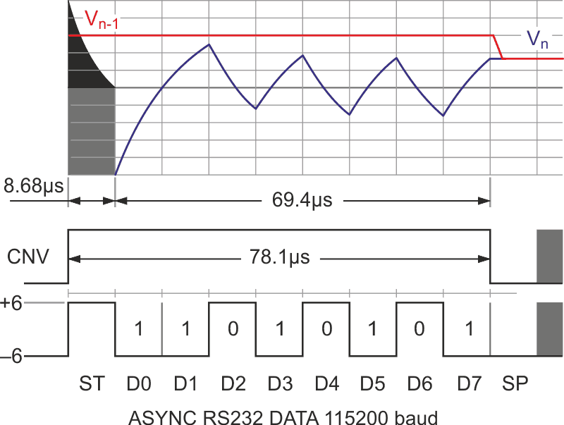
Serial transmission of bytes (at T = 8.68 µs = 115200 baud) for DA conversion follows standard UART formatting and begins with a ‘0’ start bit. This triggers the U2 555 timer via U1a and starts a

conversion cycle, driving U1b to isolate the C2 hold capacitor (which holds the previous conversion result) and connect the C1 sample capacitor to the R1 input integration resistor. Notice that

is essentially identical to the theoretical Shannon time constant of T/ln(2), and differs from the ideal by only 0.13%, assuming nominal component values.
The U1c switch converts logic levels to U4’s reference levels and applies the resulting precision 0/+5.0V bitstream to R1C1. The conversion process continues for 8T = 69.4 µs. U2 then times out, driving CNV low, causing U1b to transfer the accumulated conversion result charge on C1 to C2 and from there to U3’s voltage follower unity-gain output.
U2 then resets, arming the circuit to respond to the next data input cycle when the next start bit arrives, completing the
ripple-free conversion cycle. Higher baud rates and even faster conversion times are also easily possible.
 |
|
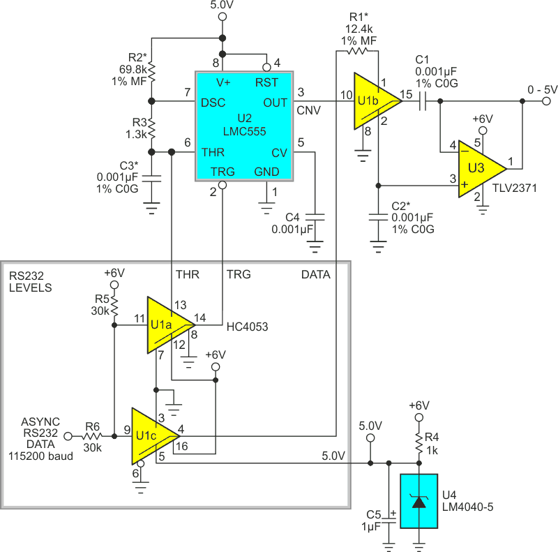
| Figure 4 | The SDD input modified for RS232 signal levels and polarity. |
Bipolar RS232 signaling, with its superior noise immunity, can also be easily accommodated by a different configuration of the U1a and U1c interface switches, as shown in Figure 4.
 |
|
| Figure 5 | The SDD analog conversion from RS232 signal levels. |
Figure 5 shows the resulting revised conversion timing.
