Readers will recognize the famous name Claude Elwood Shannon, widely renowned as the “father of information theory” and originator of many discoveries and inventions. Among these is an elegant and pioneering (First published in 1948!) design idea for a DAC called the Shannon Decoder (SD) sketched in Figure 1 (illustration modified from the Data Conversion Handbook 2005 Analog Devices).
 |
|
| Figure 1. | The Shannon decoder DAC. |
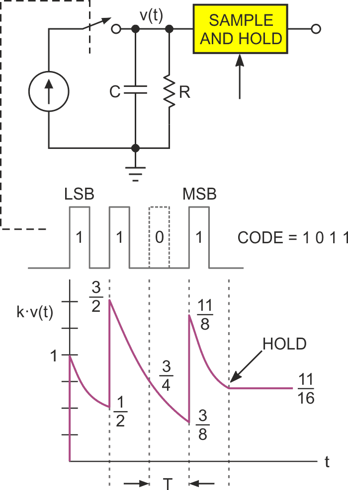
In operation, the incoming serial (LSB-first) bit string controls switch S so that a 1 bit adds a unit of charge to capacitor C while a 0 leaves it unchanged. Bits (altogether four in this simple example) arrive at time intervals T. Thus, at the end of 4T, the final voltage V accumulated on C represents the numeric content of the string. The brilliantly simple (thanks to Shannon’s genius) trick that makes V proportional to the binary number N represented by the string is
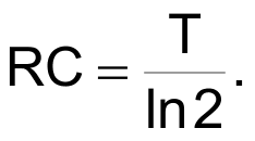
This causes exactly half the accumulated voltage on C to discharge during each interval T, providing the binary bit weights necessary for correct digital to analog conversion. The S&H then captures the final result present on C at 4T. And that’s it. We’ve completed a 4 bit DAC conversion in just four bit times using nothing but a switch, single stage RC, and S&H.
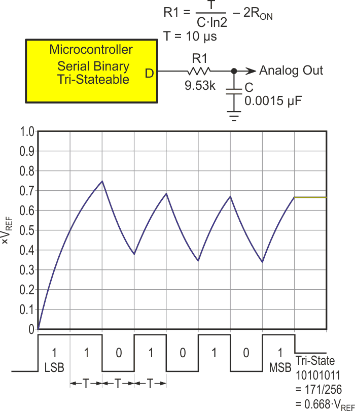
Figure 2 suggests what an 8-bit SD might look like using devices that have come along since 1948. Note that it closely resembles a basic PWM DAC, consisting only of a typical general-purpose output bit D and single-stage RC:
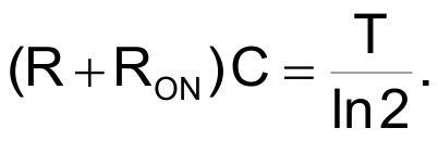
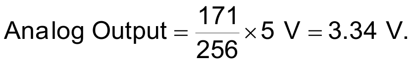
The RON term provides correction for ON resistance of the output port, typically 20 Ω to 200 Ω. We’ll see later why RON matters. Assuming an example 8 bit serial string = 10101011 = 171, T = 10 µs, C = 0.0015 µF, RON = 120 Ω, R = 9.53 kΩ, and VREF = 5 V logic supply, Analog Out (AO)
The required S&H function is provided at no cost by simply tri-stating D after Analog Out has been accumulated, allowing capacitor C to hold the final voltage and thus be its own S&H.
Previously I claimed the SD is a faster alternative to PWM. Well, is it? An 8-bit PWM has a basic period of 256 clock cycles, and in order to suppress ripple to LSB levels, the RC filter time constant needs to equal ~64 PWM periods, and will need a further Ln(256) = 5.5 time constants to settle to 1 LSB. This adds up to a total PWM DAC conversion time of 256 × 64 × 5.5 = 90,112 clock cycles to convert, filter, and settle to a final 8-bit value.
Meanwhile, the 8-bit SD does all that in only 8T cycles, apparently yielding an SD vs PWM speed ratio of 90,112/8 = 11,264 to 1, done with the same parts count as basic PWM!
But is this really a fair comparison? Well, not entirely.
First of all, regarding speed, a PWM clock cycle will typically be generated in dedicated on-chip counter-timer hardware, while the SD bit-shifting and final tri-stating of the output port bit will likely need some software interaction. This difference is likely to make the SD bit rate slower than the PWM clock. Perhaps 10x slower. Therefore, a more realistic estimate of the SD versus PWM speed ratio would probably be closer to 1,100-to-1 than 11,000-to-1.
Secondly, regarding parts count, there’s this consideration: While PWM continuously and automatically refreshes its output, the basic SD as shown in Figure 2 does not. Every few milliseconds it’s necessary for Figure 2 to run through a conversion cycle to refresh C’s charge, counteract voltage droop, and maintain a stable output. Of course, during these conversions Analog Out will be anything but stable, creating what the load will see as a momentary output glitch.
 |
|
| Figure 2. | A modern Shannon decoder implementation. |
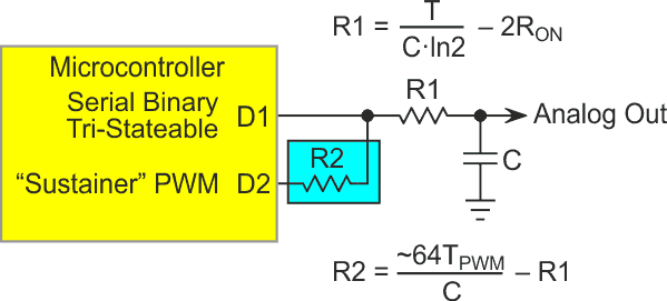
Some loads will tolerate this periodic disturbance, but many will not. Avoiding the glitch is possible, but to do so, parts count must increase. Figure 3 suggests one possible solution.
 |
|
| Figure 3. | Supplementary PWM to prevent SD output droop. |
Supplementing the speed of the SD with a “sustainer” PWM set to the same output voltage as the SD to hold the same capacitor charge that was initially (quickly) set by the SD.
This solution is still less than perfect because the large ratio between the SD and PWM time constants implies a similarly large ratio between R1 and R2, imposing a high resistance for R2 to get adequate ripple suppression and hence, a very limited steady-state drive capability for Analog Out. And of course, there’s still an output glitch whenever an SD conversion sequence sets a new output voltage.
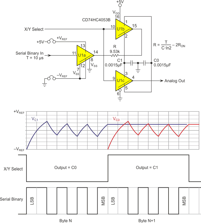
Figure 4 shows a complete remedy for these problems by implementing two S&H conversion/hold capacitors that toggle via U1c so that one provides the S&H function (C0/1 as X/Y Select = 0/1) and a constant output voltage while the other performs the next DAC conversion via U1a and U1b. Whereupon they switch roles, yada-yada and so on, etc.
 |
|
| Figure 4. | The toggling SD. |
An additional feature of Figure 4’s topology is its ability to accept reference voltage inputs (+VREF, –VREF) that are independent of logic supply and ground. This allows for better DAC accuracy than relying on the (typically limited) stability of logic power supplies, and, if –VREF is negative, a bipolar (–VREF to +VREF) output span.
The SD has inherently programmable resolution. Any length bit string (6, 10, 12, etc.) can be accommodated without any circuitry modification. Moreover, because the SD conversion time is linearly proportional to bit string length (n) while PWM conversion time is exponentially proportional to 2n, the SD’s speed advantage only gets better as string length grows.
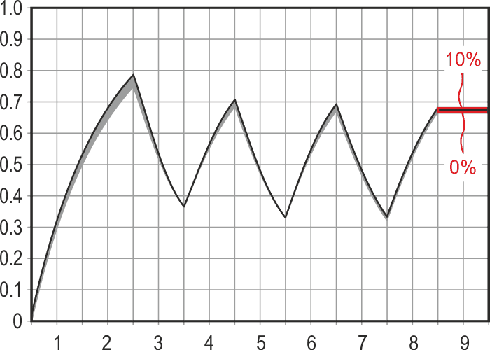
SD precision depends on an accurate match between RC time constant and bit interval T/ln(2). Differences between these two numbers will cause bit weights to differ from the correct 2.0, and monotonicity and differential linearity to consequently suffer. Use of precision metal film resistors and zero tempco C0G or NPO capacitors is therefore suggested, as well as correction of R for the impedance (RON) of switching elements in SD signal paths, as previously mentioned.
 |
|
| Figure 5. | Effect of 0% to 10% RC error. |
Figure 5 shows the effect on the conversion result of RC time constant errors from 0% (RC = 1.44269•T) to 10% (RC = 1.58696•T).
