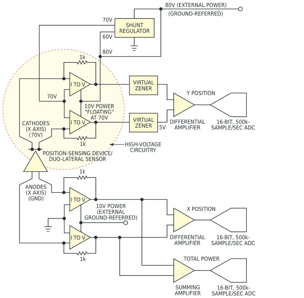
This design for a photonic switch needs more than approximately 70 V at the cathode of a duo-lateral optical position-sensing device. This voltage gets speedy response at longer wavelengths, such as 980 nm. The circuit uses fast transimpedance amps, “floated” at 70 V. Two “virtual-zener” circuits step down the high-voltage signals for subsequent processing in a ground-referred differential-amplifier stage (Figure 1). The circuit drops exactly 65.58 V dc with the component values shown, notwithstanding errors arising from op-amp offset voltages and resistor tolerances (Figure 2).
 |
|
| Figure 1. | “Virtual-zener” circuits simplify the high-voltage interface in this position-sensing system. |
 |
|
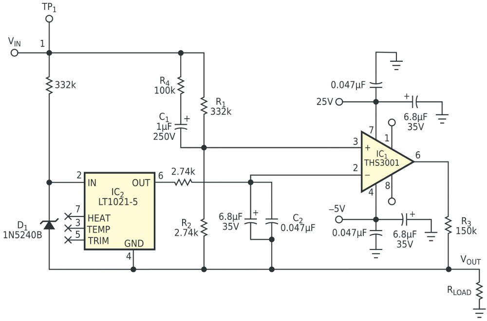
| Figure 2. | This virtual-zener circuit provides a regulated, “floating” voltage between the input and output. |
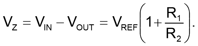
The function of the virtual-zener circuit is to provide a regulated, floating dc voltage drop between input and output. The size of the drop depends on the ratio of R1 to R2 and the magnitude of the reference voltage. The input of the circuit, nominally at 70 V dc, draws a constant 3.65 mA. The THS3001 sources or sinks this current plus any additional current as necessary, adjusting the output voltage until the voltages at its two inputs are equal. This equality occurs when
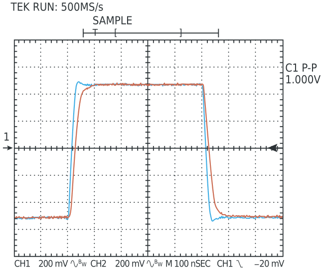
The op amp's power-supply rails and output range, along with the voltage drop across R3, limit the output-voltage compliance. C1 bypasses R1. This bypass swamps the bandwidth-reducing effect of capacitance at the noninverting input, and it greatly reduces the noise at the output. Without C1, the op amp's inherent noise would gain up by a factor of (1+R1/R2). R4 protects IC1’s noninverting input by limiting the transient current supplied by C1 during power-up and power-down. R3 and the output, RLOAD, have a similar protective effect on the inverting input, limiting any transient current in C2. R3 is necessary to ensure feedback stability of the op amp. The inclusion of this resistor is standard operating procedure for a current-feedback op amp, such as the THS3001. If you use a voltage-feedback type, you could possibly eliminate R3. Bandwidth is extremely high. Figure 3 shows the pulse response at 100 nsec per division. (Blue is the input, and red is the output.)
 |
|
| Figure 3. | The transient response of the circuit in Figure 2 is exceedingly fast. |
