This project originated from the need to produce a linear crystal-controlled ramp signal for an HP 8620C RF sweep oscillator. It is inspired by a previously published ramp generator design [1]. That design though suffered from two issues: it used a non-standard 16.384 MHz crystal oscillator and the fall/return/blanking time of the ramp was zero.
 |
|
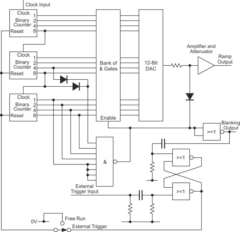
| Figure 1. | Ramp generator schematic. |
To address the first issue, the ramp generator described here uses a standard 10 MHz clock allowing it to be integrated into an existing test setup. Secondly, most equipment requires a finite time to return to its initial state before starting a new sweep. The design presented in Figures 1 and 2 (see below), overcame these issues. The ramp generator section will be described first as its requirements drove the design of the clock generator.
 |
|
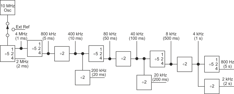
| Figure 2. | Clock generator schematic. |
Ramp Generator
The heart of the ramp generator is a 12-bit digital-to-analogue converter (DAC) driven by binary counters. The DAC is a discrete R-2R type as at the time of development a suitable IC DAC was not available. This is driven by a bank of AND gates (three 74HC08), which are in turn driver by two 74HC393 dual 4-bit binary counters – one half of one is not used. 12 bits gives a maximum possible count of 4096 states. A simplified schematic of the ramp generator is shown in Figure 1.
To define the blanking time, the DAC only outputs a ramp for the first 4,000 states. For the remaining 96 its output is held at 0 V, which is sufficient time for the HP 8620C to return to the start frequency and settle. During the ramping phase the AND gates pass the counter outputs to the DAC. During the blanking phase the AND gates are driven low, pulling the inputs to the DAC low and its output to 0 V. A two-input OR gate (two 1N4148 diodes and a resistor) and a five-input NAND gate (74HC30 with three of its input tied together) monitor the output of the counter and drive the common input of the AND gates during blanking. There is also an inverter formed from a NOR gate (74HC02) to produce a positive going blanking pulse which can be used to modulate the Z-input of an oscilloscope.
A resistor-diode switch on the output of the DAC is also enabled during the blanking phase to pull the DAC’s output to 0 V. During the ramping phase, the DAC’s output is amplified by an op-amp to provide the 10 V signal required by the HP 8620C.
The ramp generator can be switched between free-running and external trigger – it is shown in external trigger mode in Figure 1. In trigger mode, a set-reset latch composed of two NOR gates detects the rising edge of the blanking output to reset the 12-bit counter. Only when an external trigger arrives does the set-reset latch reset so that the 12-bit counter can start counting again.
Clock Generator
An internal or external 10 MHz crystal reference is divided down to 12 separate frequencies and selected by a 12-way rotary switch for feeding to the ramp generator. Since the ramp generator only produces a ramp output for the first 4,000 states instead of 4,096, the standard 2, 5, and 10 division ratios of a 74HC390 dual decade counter can be used as shown in Figure 2. The 74HC390 is composed of two separate divide-by-2 and divide-by-5 counters, which are configured as shown. The clock frequency at each output is indicated along with its corresponding sweep time in brackets.
 |
|
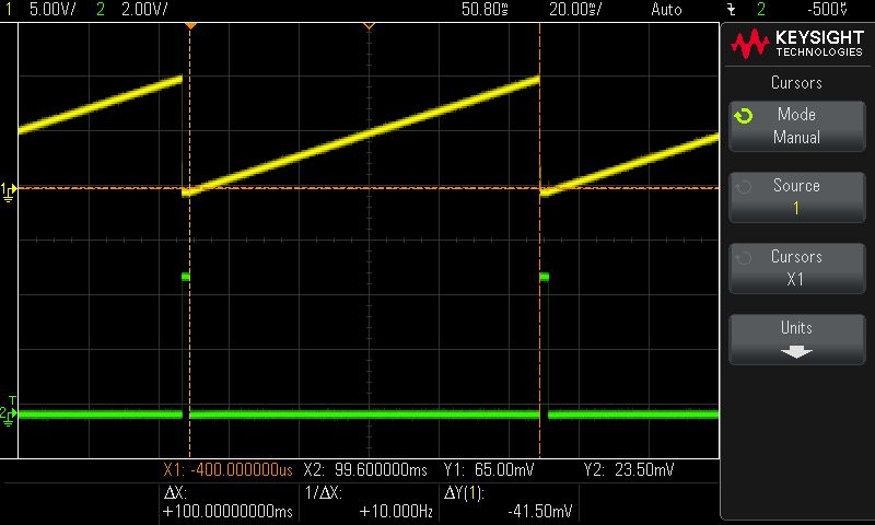
| Figure 3. | Measured waveforms: ramp output in yellow, blanking pulse in green. |
An exception to the above explanation is the 1 ms sweep time, which requires a 4 MHz clock. The first divider stage is therefore a divide-by-2.5. This is achieved by tapping off the least-significant bit of a divide-by-5 counter. For every five input pulses it produces two output pulses: 000, 001, 010, 011, 100, 000, 001, 010, 011 etc. The duty cycle of this 4 MHz clock will vary cycle-to-cycle leading to minor jitter at 1 ms sweep time, but this will only manifest itself on the least significant bit of the ramp generator counter so is not significant. Alternative divide-by-2.5s are available that have a fixed 50% duty cycle, but are more complex [2].
Results
The measured output waveforms are shown in Figure 3 for the ramp and blanking outputs, where they can be seen to have an exact period of 100 ms and the ramp has a high linearity.
The complete ramp generator was built on stripboard and housed in an equipment case with integrated power supply to form a useful piece of laboratory equipment.
References
- Neil Johnson, “Ramp Generator”, Everyday and Practical Electronics, July 1995, pp. 546-550.
- Yongping Xia, “Divide by 2.5”, Electronics World + Wireless World, December 1991, pp. 1051.
