The 8-bit resolution of a peripheral DAC (such as the ATtiny family, for instance) is often insufficient. Let’s see how the problem can be solved using on-chip resources.
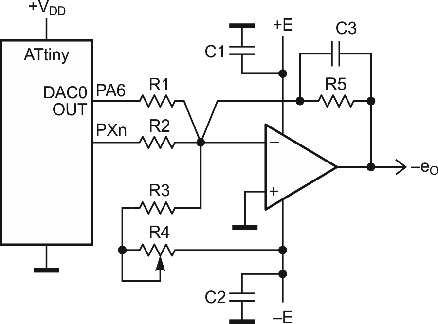
The circuit in Figure 1 shows a method to improve the resolution of a peripheral DAC. The circuit also reduces output resistance of the DAC and can reduce its offset (which is rather pronounced for ATtinyX17).
 |
|
| Figure 1. | Circuit used to improve the resolution of a peripheral DAC while also reducing the output resistance and offset of the DAC. |
This simple approach is fully static (needs no additional capacitors with their imperfections and charge refreshing), it preserves the monotonicity of the original DAC, but may require some tuning to achieve the best linearity.
To add one more bit you can use any free port of your MPU, in Figure 1, this port is marked as PXn (X = A…C, n = 0…7). (And yes, you can add more than one bit this way.)
Note: The port PXn should be configured as an output before using it as an extra bit for the DAC. Also have in mind those very useful instructions in AVR ASM, which can selectively change one bit in a row.
The bit of the PXn can be used as a new most significant bit (MSB), or a new least significant bit (LSB) – a detailed description of the last case is given below.
To maintain the integrity of the output, both the DAC0 and the PXn should have the same headroom on their outputs. The easiest way to secure this is to choose +VDD as VREF for the DAC. Of course, the value of +VDD has to be well-regulated in this case.
The op amp should provide sufficient speed and precision where the total added error at the output of the op amp is:
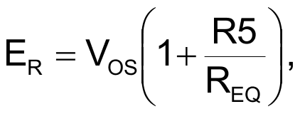
where VOS is the offset voltage of op amp and REQ = R1||R3 (approximately).
The value of ER should be at least less than 1 LSB of the modified DAC.
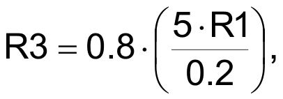
The minimal voltage on DAC0 OUT is about 0.2 V (for ATtinyX17). If this offset is okay for your application, you can exclude resistors R3 and R4, and use only one +E supply, nevertheless, the op amp should have: a rail-to-rail output, a sufficient precision, and be able to work with near zero input.
To reduce the minimal value of eO to zero, you must zero the output with the resistors R3 and R4 while DAC0 gets its zero code.
The values of all resistors can be calculated as follows:
R1 ≥ 5.6k (the requirement from the datasheet of ATtinyX17).
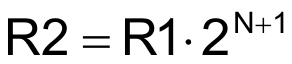
Let N bits be the original DAC resolution. Then:
(some final tuning may provide the better result).
Since the minimal voltage on DAC0 OUT is about 0.2 V,
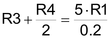
(If VDD = E = 5 V),
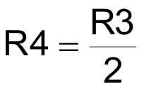
(R4 is a multi-turn pot).
The resistor R5 can easily conform the DAC output to the values expected by an application.
Some efforts may be required in the program code to synchronize the DAC0 OUT and PXn, albeit there are applications which can tolerate the de-synchronization if it is not very large (less than tens of microseconds).
Note: the output of the op amp is inverted compared to the DAC0 OUT (hence the sign “–” before eO in Figure 1). You can cope with this by adding an inverter (op amp) to the output, or by making a change in the code, which may be a better solution.
You should not expect that the previous maximal value of the conversion rate would be left unchanged. Every next added bit means a resistance that is twice as large as well as some added capacitance in the summing node.
So, the settling time will be unavoidably larger with every expansion bit added.
To reduce a parasitic capacitance in the inverting node of the op amp the resistors R1, R2, R3, and R5 should be placed close to the inverting input.
Sometimes to optimize the performance of the DAC (to compensate the amplifier), the capacitor C3 (10-40 pF) has to be connected in parallel with R5.
