Most engineers are familiar with boost converters, which step up the output voltage (VOUT) to a value that exceeds the input voltage (VIN). They are also familiar with buck-boost converters and single-ended primary-inductor converter (SEPIC), which can ensure that VOUT is above, below, or equal to VIN as needed for the receiving device.
A charge pump converter is a type of DC/DC converter that uses capacitors to raise or lower voltages. These converters often take up a smaller area, have high efficiency, and are incredibly cost-effective. They are often used in the backlight of thin-film-transistor liquid-crystal displays (TFT-LCD), optical modules, and they can drive the upper transistor (N-channel MOSFET) of a buck circuit.
Charge pumps acting as voltage doubler
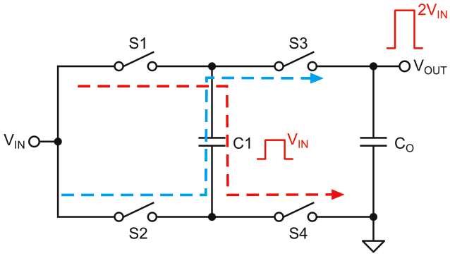
Traditionally, charge pump converters often act as voltage doubler, which charges capacitors from VIN then switches charges to ensure that VOUT is exactly double that of VIN. The basic principle is simple: charge and discharge the capacitor, then use the fact that the capacitor can store charge, isolate this charge from the charging circuit, and pass it through the discharge circuit.
For the charging phase, two of the four switches (Q1 and Q4) turn on, while the other two switches (Q2 and Q3) turn off. This allows the input to charge the capacitor (C1) (see Figure 1).
 |
|
| Figure 1. | Voltage doubler diagram. |
The conversion stage is next. In this stage, Q1 and Q4 turn off, while Q2 and Q3 turn on since the voltage across the capacitor does not change immediately. Then C1 discharges to the output capacitor (COUT). The charge transfer is accomplished through the switching transformation such that VOUT = 2×VIN.
Charge pump applications
The following sections will provide classic applications for charge pump converters.
Using a charge pump for a buck circuit's high-side MOSFET
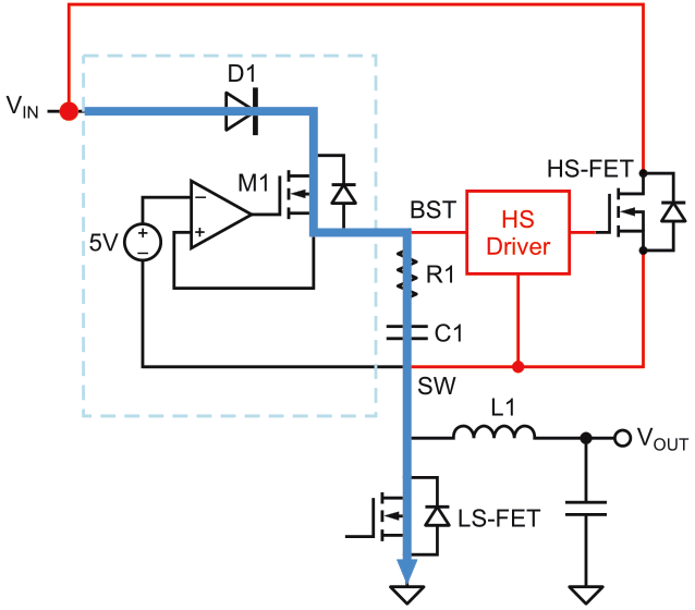
Consider a buck circuit as an example. To drive the high-side MOSFET (HS-FET) and ensure that the gate-to-source voltage (VGS) exceeds the threshold voltage (VTH), a bootstrap circuit may be required to raise the gate’s voltage.
Figure 2 shows that C1 completes the charging and discharging process within one switching cycle, which raises the gate voltage. Charge pumps are not only used by a buck converter’s bootstrap circuit to drive the HS-FET. Charge pumps can also be used to drive the HS-FET in half-bridge and full-bridge applications.
 |
|
| Figure 2. | Using a charge pump for an HS-FET. |
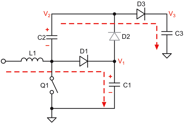
Using a charge pump in a boost circuit
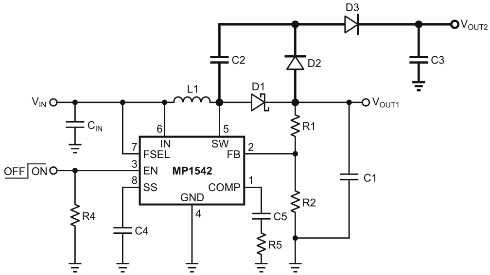
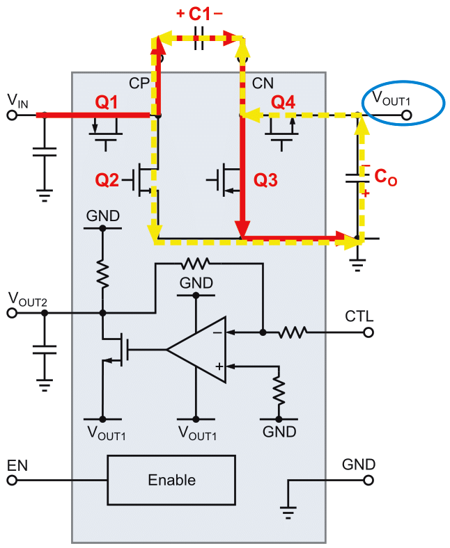
For boost applications, the boost converter’s maximum VOUT may not be able to meet the voltage specifications for certain devices, such as the VP/VN power supply in TFT-LCDs. Consider a converter that is commonly used for TFT-biased power supplies. If the output exceeds 25 V but the SW pin only supports up to 25 V, then the output is often limited.
Engineers could find an IC that can withstand higher voltages, but those ICs are less cost-effective. In this scenario, a charge pump circuit can be added (see Figure 3). With a few additional components, the boost converter has a new output (VOUT2) that is double that of the typical output voltage (VOUT1). Figure 3 shows a charge pump being used by the MP1542, a 700 kHz/ 1.3 MHz boost converter.
 |
|
| Figure 3. | A charge pump in a boost circuit. |
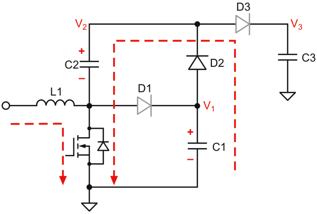
Figure 4 shows a simplified circuit based off Figure 3.
 |
|
| Figure 4. | Simplified charge pump in a boost circuit. |
Figure 5 shows the overall charging process. When Q1 turns on, C1 transfers energy to C2, which raises the voltage of C2 until the first voltage (V1) is equal to the second voltage (V2). When Q1 turns off, the second capacitor (C2) transfers energy to the output, so that the final voltage (V3) is equal to V2 + V1, or (2×V1).
 |
|
| Figure 5. | Functional diagram for simplified charge pump. |
Negative VOUT applications with a charge pump
Charge pumps can be used in applications with both positive and negative output voltages. Because they require fewer peripheral components and take up a smaller amount of space, they are popular choices for these applications.
Figure 6 shows a circuit that only needs 4 MOSFETs in the internal logic circuit so that VOUT is equal to –VIN. This circuit does not need external inductors, which reduces overall cost and simplifies the design. This compact, low-profile solution is suitable for a wide range of applications, including optical modules, RF amplifiers, and sensor power supplies.
 |
|
| Figure 6. | Charge pump in applications with negative VOUT. |
Table 1 summarizes the differences between traditional inductive DC/DC converters and capacitive DC/DC converters.
| Table 1. | Inductive DC/DC converters vs. capacitor DC/DC converters | ||||||||
|
|||||||||
Conclusion
Charge pump converters are cost-effective solutions that can effectively double an output relative to its input. Designers should choose the appropriate DC/DC converter that meets their applications requirements.
