FinFETs redefined chip design when they came onto the scene more than a decade ago. While these nonplanar transistors are still the unofficial industry standard, they may be nearing the end of their life. So, electronics engineers may need to prepare for an incoming shift.
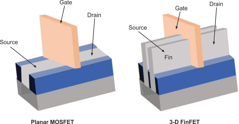
The first chips using FinFETs came out in 2011, letting semiconductors safely venture into sub-25-nm territory. At that time, this architecture was a sort of saving grace for Moore’s Law, because planar transistors led to too much current leakage for geometries below 100 nm to be sustainable (Figure 1).
 |
|
| Figure 1. | FinFETs replaced the planar transistor design with a 3D architecture to overcome the limitations of traditional planar transistors. |
However, FinFETs are now facing a problem like the planar technologies that came before them. Power leakage and signal interference issues are becoming more common obstacles as device form factors continue to shrink and performance demands rise. Consequently, many key industry players are starting to consider alternate transistor architectures.
As helpful as FinFETs are compared to their predecessors, they have severe power routing constraints at smaller geometries. Engineers typically work around these restrictions through different channel widths and spacing. That works well in many applications, but this strategy has limits of its own.
Because gates must reach the insulator between fins, sufficient space between each channel must be available. As a result, engineers can quickly run into scalability issues since there are 15 nm to 20 nm between each fin. Adding more channels inherently means adding inactive areas, leading to a tradeoff between current routing and physical space.
Gate-all-around (GAA) transistors
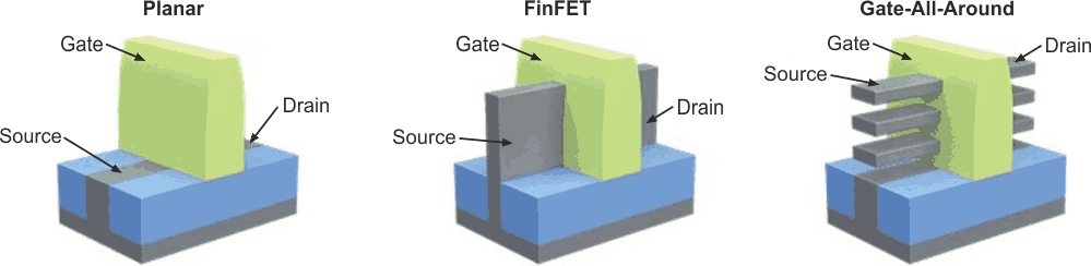
A potential solution has emerged in the form of gate-all-around (GAA) transistors. GAA architecture reverts to planar form factors, but instead of using a flat channel flush with the insulator, it uses silicon ribbons surrounded by the gate on all sides.
Just as FinFETs let engineers place multiple fins next to each other, GAAs enable vertical channel stacking. Notably, this method still requires space between each ribbon. However, because it capitalizes on verticality, each one can cover a longer horizontal space. Alternatively, engineers could design taller but narrower transistors to leave more room on the chip for other components.
Another key advantage of GAA design is that the gate contacts the channel on all four sides. Consequently, it provides more control over higher currents, just as FinFETs did in relation to conventional planar architectures (Figure 2).
 |
|
| Figure 2. | In GAA transistor structure, the gate can come into contact with the channel on all sides, which makes continuous scaling possible. |
GAAs are still relatively new, but they’re already showing signs of becoming standard. Samsung led the charge, announcing a switch to GAAFETs in 2022. Intel, which put FinFETs on the map, will release its GAA technology later in 2024, along with a backside power technology.
Several obstacles remain. Some reports hold that Samsung is struggling to achieve high yields with its GAAFET technology. Other foundries have more long-term release windows for their GAA chips, so whether GAA technology will be able to overcome these challenges remains unclear.
Despite these road bumps, the industry is clearly moving toward GAAs. So, electronics designers should familiarize themselves with this technology before the shift happens to adapt to the changing market.
Transition on the gate
Just as FinFETs redefined semiconductor architecture in the 2010s, GAAFETs could do the same within the next decade. While much of this transition is still up in the air, most signs seem to be pointing that way.
Electronics engineering is a continually evolving field. Therefore, engineers must stay abreast of developments like this to ensure they can capitalize on the innovations that revolutionize the industry.
