When building AVR DDS2 signal generator there were lots of discussions about signal conditioning in analog part of device. First argument was that LM358 wasn’t the best choice for this purpose. Another one pointed to sine wave that weren’t smooth enough.
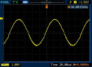
As you can see there are some dents on it. Other waveforms also are distorted especially when higher voltages are selected. This definitely asks for better analog part. Some people suggested to replace LM358 with OPA2134, but it seems to be quite expensive choice. In my opinion low noise general purpose op-amp can be great too. I’m gonna give a try to Texas Instruments TL074 low noise op-amp. It is low power, high slew rate (13V/us) IC – almost five times faster than LM358 and for same reasonable price.
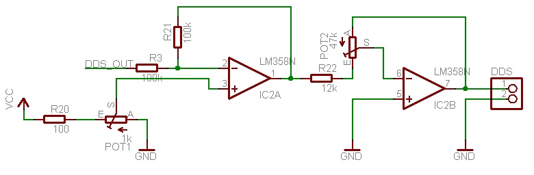
If we look at DDS2 signal generator offset and gain control circuit we can see that there is a problem in it. We regulate offset before amplitude control – normally offset should be regulated after amplifying signal. And third problem is that offset can be regulated in small interval – in 5V range while we could do this in -12V … +12V range. Lets redesign analog part so it would give better result.
Zeroing offset voltage
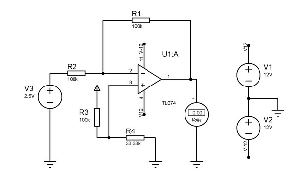
First of all offset control we can slightly modify first stage so that offset voltage of signal would be set to 0. For instance if we are generating sine-wave on DAC we get maximum 2.5V amplitude signal with 2.5V DC offset. Instead of using POT1 we can calculate resistor divider so that on output we get 0V offset. We assume that all signals coming out of microcontroller have offset 2.5V (when VCC=5V), then we can model following circuit:
Calculating is easy:
We know that source voltage is Vs=2.5V. Output voltage is Vo=0V. We need gain 1 (-1 for inverting amp). So at inverting op – amp input we get voltage:
![]()
From from operational amp analysis we know that V- = V+ and currents to both inputs are equal to zero (I- = I+ = 0A). Then We must get 1.25V at V3. so we need to select voltage divider to scale voltage from 5V to 1.25. To do so we chose one fixed resistor value R3 to be 100kOhms and then we calculate R4:
![]()
evaluate R4:
![]()
We can get 33.33kΩ by connecting two resistors in series: 33kΩ + 330Ω that will give resulting voltage close enough to 0V.
Optional filter stage
In the next stage of analog part we are going to add a filter. Since DDS signal generator is capable of outputting various types of signals we don’t want it to be hardwired. For instance if we generate sine wave the we could use filter to make it more smooth while on square wave it would have negative effect by rounding the shape. For this we can add a bypass switch that would allow to insert or bypass filter on demand. What filter are we going to use for this purpose. Since we have plenty of op-amps on TL074 we can make an active filter.
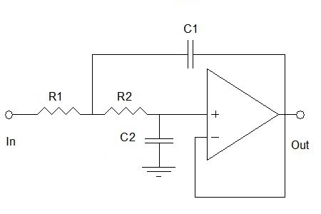
I find Butterworth (Sallen – Key) low pass filter quite handy since it gives flattest response in band. Lets select parameters for this filter. DDS generator in our case isn’t going to exceed 100kHz frequency. Also we want attenuation in this up to roll – off frequency close 0dB. So lets increase roll-off frequency up to 200kHz. This value we are going to use while calculating.
Resistor and capacitor values of filter can be determined with these simple rules:
R1 = R2, C1 = 2·C2
If we select R2 = R1 = 33k (have plenty of these)
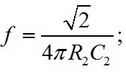
then we can calculate C2 as follows:
![]()
so standard value of C1 = 33pF.
You can check calculations on line here.
Part 2 - Signal Amplitude Gain Control, Signal Offset Regulation, Putting it All Together