Evaluating analog switches, multiplexers, operational amplifiers, and other ICs poses challenges to IC-test engineers. A typical test scenario requires application of a test or forcing voltage to a device's input and measurement of any resultant leakage and offset currents, often at levels of 1 pA or less. In contrast to slow and expensive commercially available automated testers, the low-power measurement circuit in figure 1, figure 2, and figure 3 can force a wide range of test voltages and offer fast settling to maximize device-test throughput. Extensive use of surface-mounted components minimizes its pc-board-space requirements and allows packaging of multiple measurement circuits close to the test fixture.
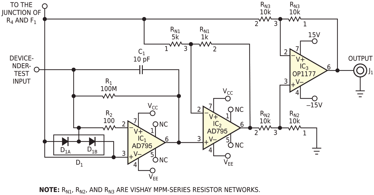
The circuit comprises a forcing-voltage buffer/amplifier, a floating-rail power supply, and an IVC (current-to-voltage converter). Applying a forcing voltage to a device under test induces leakage current, which the circuit converts to an output voltage proportional to the leakage current. In a conventional IVC, the current to be measured develops a voltage across a shunt resistor. The IVC uses a feedback-ammeter topology in which operational amplifier IC1, an Analog Devices AD795, subtracts an unknown current from a feedback current and delivers an output voltage proportional to the unknown current (Figure 1).
 |
|
| Figure 1. | This IVC uses a feedback-ammeter topology, which subtracts an unknown current from a feedback current and delivers an output voltage proportional to the unknown current |
In this design, the input's dc resistance consists mostly of R2 and IC1’s effective input resistance, or slightly more than 100 Ω at dc. At frequencies in the power-line range of 50 to 300 Hz, the circuit's ac impedance averages approximately 10 kΩ, or 1000 times less than a typical shunt-resistance IVC's input resistance of approximately 10 MΩ. The circuit's 100-MΩ feedback resistor, R1, provides a current-to-voltage-conversion ratio that exceeds the shunt-conversion ratio by a factor of 10. This design settles much faster and provides better interference rejection at power-line frequencies than shunt converters. It also reduces unwanted voltage-divider effects when testing operational amplifiers' input currents.
R1 produces a current-to-voltage-conversion ratio of 100 µV/pA. Amplifier IC2, an AD795, provides an additional voltage gain of 0, boosting the ratio to 1 mV/pA and reducing the effect of errors that differential amplifier IC3’s CMRR (common-mode-rejection ratio) introduces. Differential amplifier IC3, an OP1177, subtracts the forcing voltage from the IVC's output and provides a ground-referenced output signal.
A back-to-back pair of BAV199 diodes, D1A and D1B, protects IC1 from voltage overloads by shunting high currents to the forcing-voltage amplifier, IC4, and its protective fuse, F1. When the forcing voltage rapidly slews from one value to another, the diodes greatly improve the IVC's settling time by providing high-drive currents during high-slew-rate intervals.
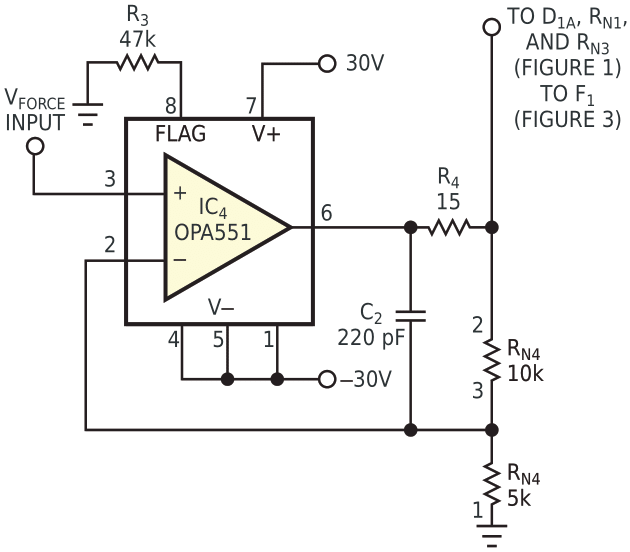
Operating from ±30 V supply rails, a lightly compensated, gain-of-three, high-voltage OPA551 amplifier, IC4, derives forcing voltages as high as ±22 V from ordinary ATE (automatic-test-equipment) voltages of ±7 V (Figure 2). In case of a catastrophically shorted device under test, fuse F1 prevents further damage by limiting fault current from IC4, which can deliver as much as 380 mA of short-circuit current.
 |
|
| Figure 2. | A gain-of-three high-voltage amplifier derives forcing voltages as high as ±22 V from voltages of ±7 V from test equipment. |
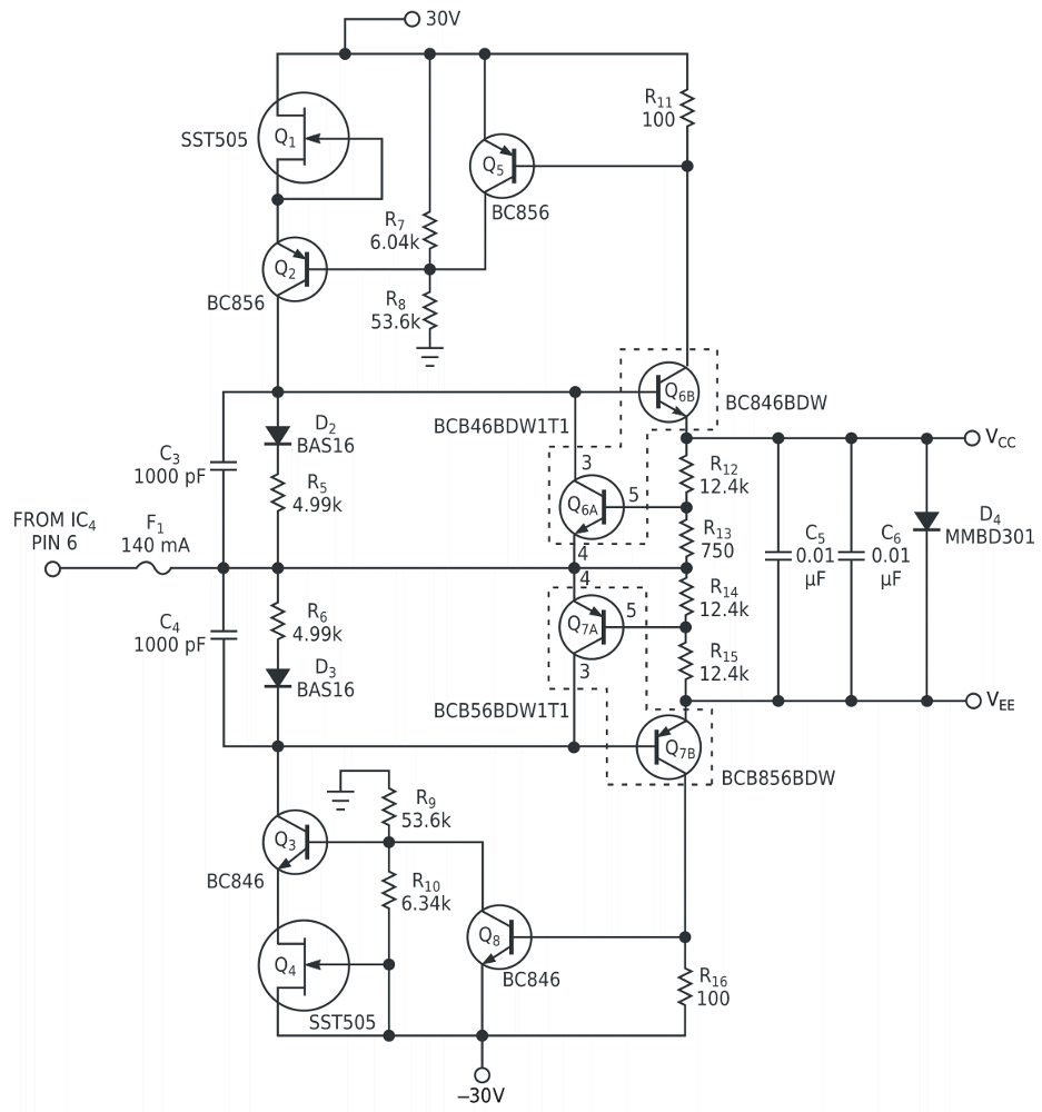
The output of IC4 also drives a regulator circuit that produces ±5 V floating-power-supply voltages referenced to the test-input forcing voltage (Figure 3). This part of the circuit dissipates less than 100 mW of power with ±30 V supplies. Vishay/Siliconix SST505 JFET constant-current regulator “diodes” Q1 and Q4 provide 1-mA constant-current sources, which transistors Q2 and Q3 buffer. Each current-regulator diode carries a 45 V maximum rating, and the buffers provide overvoltage protection by limiting the voltages applied across the diodes to approximately 3 V.
 |
|
| Figure 3. | This floating-regulator circuit produces ±5 V floating-power-supply voltages VCC and VEE referenced to the test input’s forcing voltage. |
Applying 1 mA to resistors R5 and R6 develops the ±5 V rail voltages. Diodes D2 and D3 compensate for the base-emitter-voltage drops across emitter followers Q6B and Q7B. Transistors Q6A and Q7A provide overvoltage protection when a defective device under test short-circuits its power supply to the IVC's input node. Transistors Q5 and Q8 limit the floating supplies' output currents by shunting the current diodes. Diode D4 protects against polarity inversion of the floating-supply rails during unusual start-up conditions.
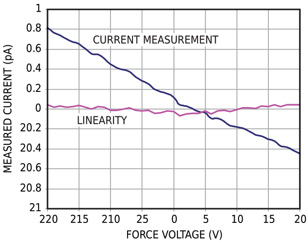
In operation, the circuit delivers an output of 0.999 V/nA over a ±4-nA full-scale input range at an effective transresistance of 1 GΩ. The circuit's output offset corresponds to approximately 143 fA. Beyond the forced-voltage span of ±22 V, the floating-supply-rail voltages begin to saturate, the input-CMRR limitations of IC3 become evident, and the IVC's output voltage becomes nonlinear. Figure 4 shows the circuit's current-measurement error of –31 fA/V from the circuit's unloaded output over a ±20 V forcing-voltage span. The differential amplifier comprising IC3, RN2, and RN3 contributes most of the circuit's gain, and IC1’s low input-bias current contributes to the low offset error. Output linearity over the ±20 V forcing-voltage range averages 111 fA p-p.
 |
|
| Figure 4. | Over a ±20 V forcing-voltage span, the circuit produces an unloaded- output current-measurement error of –31 fA/V. |
The circuit's slew-rate capability varies considerably, but in general the output faithfully slews the entire 40 V forcing-voltage span in 100 µsec or less as D1 drives the device under test. Once the high-slew period completes, the IVC comes out of saturation, and its output becomes an exponential voltage with a time constant of 1 msec. The output settles to 100 fA in approximately 10.6 msec. Under no-load conditions, the circuit consumes approximately 10.2 mA from the ±30 V supplies and 400 µA from the ±15 V supplies. The prototype circuit's layout occupies approximately 1.5 in.2 on a single-sided pc board, and placing components on both sides of a double-sided board would reduce the area to 1 in.2 For best performance, the layout must include guard rings around the input terminal and all traces attached to Pin 2 of IC1. The circuit's size allows its placement on a device-under-test fixture to minimize lead lengths and power-line-induced electromagnetic interference. Although able to measure currents as small as 1 pA, the circuit can accommodate larger currents by reducing the value of R1.
