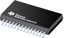
Datasheet Texas Instruments CDC536DBR
| Manufacturer | Texas Instruments |
| Series | CDC536 |
| Part Number | CDC536DBR |

3.3V PLL Clock Driver with 1/2x, 1x and 2x Frequency Options 28-SSOP
Datasheets
CDC536: 3.3-V PLL Clock Driver With 3-State Outputs datasheet
PDF, 322 Kb, Revision: G, File published: Jul 8, 2004
Extract from the document
Status
| Lifecycle Status | Active (Recommended for new designs) |
| Manufacture's Sample Availability | No |
Packaging
| Pin | 28 |
| Package Type | DB |
| Industry STD Term | SSOP |
| JEDEC Code | R-PDSO-G |
| Package QTY | 2000 |
| Carrier | LARGE T&R |
| Device Marking | CDC536 |
| Width (mm) | 5.3 |
| Length (mm) | 10.2 |
| Thickness (mm) | 1.95 |
| Pitch (mm) | .65 |
| Max Height (mm) | 2 |
| Mechanical Data | Download |
Parametrics
| Absolute Jitter (Peak-to-Peak Cycle or Period Jitter) | 200 ps |
| Number of Outputs | 6 |
| Operating Frequency Range(Max) | 100 MHz |
| Operating Frequency Range(Min) | 25 MHz |
| Package Group | SSOP |
| Package Size: mm2:W x L | 28SSOP: 80 mm2: 7.8 x 10.2(SSOP) PKG |
| Rating | Catalog |
| VCC | 3.3 V |
| t(phase error) | 500 ps |
| tsk(o) | 500 ps |
Eco Plan
| RoHS | Compliant |
Application Notes
- Application and Design Considerations for CDC5xx Phase-Lock Loop Clock DriversPDF, 101 Kb, File published: Apr 1, 1996
Today?s high-speed system designs require stringent propagation and skew parameters to maintain desired system performance. TI developed the CDC5XX platform of PLL clock drivers to meet the need for high-performance clock system components. This document describes the features and functions of the CDC5XX and discusses design considerations and configurations for the CDC586, CDC582, and CDC2582 clo
Model Line
Series: CDC536 (4)
- CDC536DB CDC536DBG4 CDC536DBR CDC536DBRG4
Manufacturer's Classification
- Semiconductors > Clock and Timing > Clock Buffers > Zero Delay Buffers