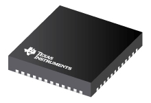
Datasheet Texas Instruments CDCE62005
| Manufacturer | Texas Instruments |
| Series | CDCE62005 |

5/10 Outputs Clock Generator/Jitter Cleaner with Integrated Dual VCO
Datasheets
CDCE62005 3:5 Clock Generator, Jitter Cleaner with Integrated Dual VCOs datasheet
PDF, 2.9 Mb, Revision: G, File published: May 23, 2016
Extract from the document
Status
| CDCE62005RGZR | CDCE62005RGZT | |
|---|---|---|
| Lifecycle Status | Active (Recommended for new designs) | Active (Recommended for new designs) |
| Manufacture's Sample Availability | No | Yes |
Packaging
| CDCE62005RGZR | CDCE62005RGZT | |
|---|---|---|
| N | 1 | 2 |
| Pin | 48 | 48 |
| Package Type | RGZ | RGZ |
| Industry STD Term | VQFN | VQFN |
| JEDEC Code | S-PQFP-N | S-PQFP-N |
| Package QTY | 2500 | 250 |
| Carrier | LARGE T&R | SMALL T&R |
| Device Marking | 62005 | 62005 |
| Width (mm) | 7 | 7 |
| Length (mm) | 7 | 7 |
| Thickness (mm) | .9 | .9 |
| Pitch (mm) | .5 | .5 |
| Max Height (mm) | 1 | 1 |
| Mechanical Data | Download | Download |
Parametrics
| Parameters / Models | CDCE62005RGZR | CDCE62005RGZT |
|---|---|---|
| Input Level | LVPECL, LVDS, LVCMOS | LVPECL, LVDS, LVCMOS |
| Number of Outputs | 5 | 5 |
| Operating Temperature Range, C | -40 to 85 | -40 to 85 |
| Output Frequency(Max), MHz | 1175 | 1175 |
| Output Frequency(Min), MHz | 4.25 | 4.25 |
| Output Level | LVPECL, LVDS, LVCMOS | LVPECL, LVDS, LVCMOS |
| Package Group | VQFN | VQFN |
| Package Size: mm2:W x L, PKG | 48VQFN: 49 mm2: 7 x 7(VQFN) | 48VQFN: 49 mm2: 7 x 7(VQFN) |
| Programmability | EEPROM, SPI | EEPROM, SPI |
| Special Features | Design Tool Available | Design Tool Available |
| VCC Core, V | 3.3 | 3.3 |
| VCC Out, V | 3.3 | 3.3 |
Eco Plan
| CDCE62005RGZR | CDCE62005RGZT | |
|---|---|---|
| RoHS | Compliant | Compliant |
Application Notes
- CDCE62005 Application ReportPDF, 296 Kb, File published: Nov 21, 2008
- LAN & WAN clock generation and muxing using the CDCE62005PDF, 2.9 Mb, File published: Nov 19, 2008
- CDCE62005 Phase Noise and Jitter Cleaning PerformancePDF, 2.5 Mb, File published: Sep 5, 2008
This application report presents phase noise data taken on the Texas Instruments' CDCE62005 jitter cleaner and synchronizer PLL. The phase noise performance of the CDCE62005 depends both on the phase noise of the reference clock and the CDCE62005 itself. This application report shows the phase noise performance at the most popular CDMA frequencies and helps the user to choose the right clocking so - Phase Noise Performance and Loop Bandwidth Optimization of CDCE62005PDF, 556 Kb, File published: Aug 11, 2011
- Clocking Design Guidelines: Unused PinsPDF, 158 Kb, File published: Nov 19, 2015
- Effects of Clock Spur on High Speed DAC Performance (Rev. A)PDF, 828 Kb, Revision: A, File published: May 18, 2015
- Effects of Clock Noise on High Speed DAC PerformancePDF, 674 Kb, File published: Nov 8, 2012
- CDCE62005 as Clock Solution for High-Speed ADCsPDF, 805 Kb, File published: Sep 4, 2008
TI has introduced a family of devices well-suited to meet the demands for high-speed ADC devices such as the ADS5527 which is capable of sampling up to 210 MSPS. To realize the full potential of these high-performance products it is imperative to provide a low phase noise clock source. The CDCE62005 clock synthesizer chip offers a real-world clocking solution to meet these stringent requirements
Model Line
Series: CDCE62005 (2)
Manufacturer's Classification
- Semiconductors> Clock and Timing> Clock Generators> Low Jitter <1psec RMS