Datasheet Texas Instruments CDCL6010
| Manufacturer | Texas Instruments |
| Series | CDCL6010 |
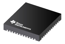
1.8V 11-Outputs Clock Multiplier, Distributor, Jitter Cleaner and Buffer
Datasheets
1.8V, 11 Output Clock Multiplier, Distributor, Jitter Cleaner & Buffer datasheet
PDF, 878 Kb, Revision: B, File published: Mar 28, 2011
Extract from the document
Status
| CDCL6010RGZR | CDCL6010RGZRG4 | CDCL6010RGZT | CDCL6010RGZTG4 | |
|---|---|---|---|---|
| Lifecycle Status | Active (Recommended for new designs) | Active (Recommended for new designs) | Active (Recommended for new designs) | Active (Recommended for new designs) |
| Manufacture's Sample Availability | Yes | No | No | No |
Packaging
| CDCL6010RGZR | CDCL6010RGZRG4 | CDCL6010RGZT | CDCL6010RGZTG4 | |
|---|---|---|---|---|
| N | 1 | 2 | 3 | 4 |
| Pin | 48 | 48 | 48 | 48 |
| Package Type | RGZ | RGZ | RGZ | RGZ |
| Industry STD Term | VQFN | VQFN | VQFN | VQFN |
| JEDEC Code | S-PQFP-N | S-PQFP-N | S-PQFP-N | S-PQFP-N |
| Package QTY | 2500 | 2500 | 250 | |
| Carrier | LARGE T&R | LARGE T&R | SMALL T&R | |
| Device Marking | 6010 | CDCL | 6010 | |
| Width (mm) | 7 | 7 | 7 | 7 |
| Length (mm) | 7 | 7 | 7 | 7 |
| Thickness (mm) | .9 | .9 | .9 | .9 |
| Pitch (mm) | .5 | .5 | .5 | .5 |
| Max Height (mm) | 1 | 1 | 1 | 1 |
| Mechanical Data | Download | Download | Download | Download |
Parametrics
| Parameters / Models | CDCL6010RGZR | CDCL6010RGZRG4 | CDCL6010RGZT | CDCL6010RGZTG4 |
|---|---|---|---|---|
| Approx. Price (US$) | 8.03 | 1ku | |||
| Input Level | Crystal, LVCMOS | Crystal, LVCMOS | Crystal, LVCMOS | Crystal LVCMOS |
| No. of Outputs | 2 | |||
| Number of Outputs | 2 | 2 | 2 | |
| Operating Temperature Range, C | -40 to 85 | -40 to 85 | -40 to 85 | |
| Operating Temperature Range(C) | -40 to 85 | |||
| Output Frequency(Max), MHz | 683.28 | 683.28 | 683.28 | |
| Output Frequency(Max)(MHz) | 683.28 | |||
| Output Frequency(Min), MHz | 15 | 15 | 15 | |
| Output Frequency(Min)(MHz) | 15 | |||
| Output Level | LVPECL, LVDS, LVCMOS | LVPECL, LVDS, LVCMOS | LVPECL, LVDS, LVCMOS | LVPECL LVDS LVCMOS |
| Package Group | VQFN | VQFN | VQFN | VQFN |
| Package Size: mm2:W x L, PKG | 48VQFN: 49 mm2: 7 x 7(VQFN) | 48VQFN: 49 mm2: 7 x 7(VQFN) | 48VQFN: 49 mm2: 7 x 7(VQFN) | |
| Package Size: mm2:W x L (PKG) | 48VQFN: 49 mm2: 7 x 7(VQFN) | |||
| Programmability | Pin configuration | Pin configuration | Pin configuration | Pin configuration |
| Special Features | I2C | I2C | I2C | I2C |
| VCC Core, V | 3.3 | 3.3 | 3.3 | |
| VCC Core(V) | 3.3 | |||
| VCC Out, V | 3.3 | 3.3 | 3.3 | |
| VCC Out(V) | 3.3 |
Eco Plan
| CDCL6010RGZR | CDCL6010RGZRG4 | CDCL6010RGZT | CDCL6010RGZTG4 | |
|---|---|---|---|---|
| RoHS | Compliant | Compliant | Compliant | Not Compliant |
| Pb Free | No |
Application Notes
- CDCL6010 as a Frequency Synthesizer and Jitter CleanerPDF, 585 Kb, File published: Mar 14, 2007
This application report provides general guidelines for using the TI 1.8V LVDS/LVCMOS clock receiver CDCL6010 as a frequency synthesizer and/or jitter cleaner. This report reviews the basic device functionality and most efficient methods of use. The document also includes a detailed discussion of generating multiple frequencies with a common input frequency as well as a practical example of this
Model Line
Series: CDCL6010 (4)
Manufacturer's Classification
- Semiconductors> Clock and Timing> Clock Generators> General Purpose