Datasheet Texas Instruments TMS320VC5510A
| Manufacturer | Texas Instruments |
| Series | TMS320VC5510A |
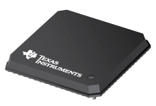
Fixed-Point Digital Signal Processors
Datasheets
TMS320VC5510/5510A Fixed-Point Digital Signal Processors datasheet
PDF, 1.3 Mb, Revision: O, File published: Sep 24, 2007
Extract from the document
Prices
Status
| TMS320SP103AZGW2 | TMS320VC5510AGGW1 | TMS320VC5510AGGW2 | TMS320VC5510AGGWA1 | TMS320VC5510AGGWA2 | TMS320VC5510AZGW1 | TMS320VC5510AZGW2 | TMS320VC5510AZGWA1 | TMS320VC5510AZGWA2 | |
|---|---|---|---|---|---|---|---|---|---|
| Lifecycle Status | Active (Recommended for new designs) | Active (Recommended for new designs) | Active (Recommended for new designs) | Active (Recommended for new designs) | Active (Recommended for new designs) | Active (Recommended for new designs) | Active (Recommended for new designs) | Active (Recommended for new designs) | Active (Recommended for new designs) |
| Manufacture's Sample Availability | No | No | No | No | No | No | No | No | Yes |
Packaging
| TMS320SP103AZGW2 | TMS320VC5510AGGW1 | TMS320VC5510AGGW2 | TMS320VC5510AGGWA1 | TMS320VC5510AGGWA2 | TMS320VC5510AZGW1 | TMS320VC5510AZGW2 | TMS320VC5510AZGWA1 | TMS320VC5510AZGWA2 | |
|---|---|---|---|---|---|---|---|---|---|
| N | 1 | 2 | 3 | 4 | 5 | 6 | 7 | 8 | 9 |
| Pin | 240 | 240 | 240 | 240 | 240 | 240 | 240 | 240 | 240 |
| Package Type | ZGW | GGW | GGW | GGW | GGW | ZGW | ZGW | ZGW | ZGW |
| Industry STD Term | BGA MICROSTAR | BGA MICROSTAR | BGA MICROSTAR | BGA MICROSTAR | BGA MICROSTAR | BGA MICROSTAR | BGA MICROSTAR | BGA MICROSTAR | BGA MICROSTAR |
| JEDEC Code | S-PBGA-N | S-PBGA-N | S-PBGA-N | S-PBGA-N | S-PBGA-N | S-PBGA-N | S-PBGA-N | S-PBGA-N | S-PBGA-N |
| Package QTY | 126 | 1 | 126 | 126 | 126 | 126 | 126 | 126 | 126 |
| Carrier | JEDEC TRAY (5+1) | JEDEC TRAY (5+1) | JEDEC TRAY (5+1) | JEDEC TRAY (5+1) | JEDEC TRAY (5+1) | JEDEC TRAY (5+1) | JEDEC TRAY (5+1) | JEDEC TRAY (5+1) | |
| Device Marking | VC5510AZGW2 | VC5510AGGW1 | VC5510AGGW2 | TMS320 | TMS320 | VC5510AZGW1 | TMS320 | VC5510AZGWA1 | VC5510AZGWA2 |
| Width (mm) | 15 | 15 | 15 | 15 | 15 | 15 | 15 | 15 | 15 |
| Length (mm) | 15 | 15 | 15 | 15 | 15 | 15 | 15 | 15 | 15 |
| Thickness (mm) | .9 | .9 | .9 | .9 | .9 | .9 | .9 | .9 | .9 |
| Pitch (mm) | .8 | .8 | .8 | .8 | .8 | .8 | .8 | .8 | .8 |
| Max Height (mm) | 1.4 | 1.4 | 1.4 | 1.4 | 1.4 | 1.4 | 1.4 | 1.4 | 1.4 |
| Mechanical Data | Download | Download | Download | Download | Download | Download | Download | Download | Download |
Parametrics
| Parameters / Models | TMS320SP103AZGW2 | TMS320VC5510AGGW1 | TMS320VC5510AGGW2 | TMS320VC5510AGGWA1 | TMS320VC5510AGGWA2 | TMS320VC5510AZGW1 | TMS320VC5510AZGW2 | TMS320VC5510AZGWA1 | TMS320VC5510AZGWA2 |
|---|---|---|---|---|---|---|---|---|---|
| Applications | Audio,Automotive,Communications and Telecom,Consumer Electronics,Industrial | Audio,Automotive,Communications and Telecom,Consumer Electronics,Industrial | Audio,Automotive,Communications and Telecom,Consumer Electronics,Industrial | Audio,Automotive,Communications and Telecom,Consumer Electronics,Industrial | Audio,Automotive,Communications and Telecom,Consumer Electronics,Industrial | Audio,Automotive,Communications and Telecom,Consumer Electronics,Industrial | Audio,Automotive,Communications and Telecom,Consumer Electronics,Industrial | Audio,Automotive,Communications and Telecom,Consumer Electronics,Industrial | Audio,Automotive,Communications and Telecom,Consumer Electronics,Industrial |
| DRAM | SDRAM | SDRAM | SDRAM | SDRAM | SDRAM | SDRAM | SDRAM | SDRAM | SDRAM |
| DSP | 1 C55x | 1 C55x | 1 C55x | 1 C55x | 1 C55x | 1 C55x | 1 C55x | 1 C55x | 1 C55x |
| DSP MHz, Max. | 160,200 | 160,200 | 160,200 | 160,200 | 160,200 | 160,200 | 160,200 | 160,200 | 160,200 |
| HPI | 1 16-bit HPI | 1 16-bit HPI | 1 16-bit HPI | 1 16-bit HPI | 1 16-bit HPI | 1 16-bit HPI | 1 16-bit HPI | 1 16-bit HPI | 1 16-bit HPI |
| McBSP | 3 | 3 | 3 | 3 | 3 | 3 | 3 | 3 | 3 |
| Operating Systems | DSP/BIOS,VLX | DSP/BIOS,VLX | DSP/BIOS,VLX | DSP/BIOS,VLX | DSP/BIOS,VLX | DSP/BIOS,VLX | DSP/BIOS,VLX | DSP/BIOS,VLX | DSP/BIOS,VLX |
| Operating Temperature Range, C | -40 to 85,0 to 85 | -40 to 85,0 to 85 | -40 to 85,0 to 85 | -40 to 85,0 to 85 | -40 to 85,0 to 85 | -40 to 85,0 to 85 | -40 to 85,0 to 85 | -40 to 85,0 to 85 | -40 to 85,0 to 85 |
| Rating | Catalog | Catalog | Catalog | Catalog | Catalog | Catalog | Catalog | Catalog | Catalog |
Eco Plan
| TMS320SP103AZGW2 | TMS320VC5510AGGW1 | TMS320VC5510AGGW2 | TMS320VC5510AGGWA1 | TMS320VC5510AGGWA2 | TMS320VC5510AZGW1 | TMS320VC5510AZGW2 | TMS320VC5510AZGWA1 | TMS320VC5510AZGWA2 | |
|---|---|---|---|---|---|---|---|---|---|
| RoHS | Compliant | See ti.com | See ti.com | See ti.com | See ti.com | Compliant | Compliant | Compliant | Compliant |
Application Notes
- Using the Power Scaling Library (Rev. A)PDF, 402 Kb, Revision: A, File published: Sep 30, 2004
Power consumption is a key concern for embedded system developers. By developing low-power solutions, developers can deliver products that have longer battery life. One technique that can be used to save power is frequency and voltage scaling of the processor.Since the power consumption of a DSP is proportional to the system clock switching speed, running the device at the lowest possible fre - Interfacing TMS320VC5510 to SBSRAM (Rev. A)PDF, 140 Kb, Revision: A, File published: Jun 16, 2003
The TMS320C55xв„ў(C55xв„ў) External Memory Interface (EMIF) supports a glueless interface to high-density and high-speed synchronous burst static random access memories (SBSRAM). For clocking SBSRAMs, the EMIF can operate at numerous C55x DSP CPU clock output frequency multiples. Examples are given for system-level connection and register configuration for the different types of SBSRAM mem - Using the TMS320VC5510 Bootloader (Rev. C)PDF, 269 Kb, Revision: C, File published: Oct 19, 2004
This document describes the features of the on-chip bootloader provided with the TMS320VC5510 Digital Signal Processor (DSP). Included are descriptions of each of the available boot modes and any interfacing requirements associated with them, instructions on generating the boot table, and information on migration from the prototype (TMX320VC5510, revision 1.x) to the production (TMS320VC5510) boot - TMS320VC5510/5510A Hardware Designer's Resource Guide (Rev. A)PDF, 100 Kb, Revision: A, File published: Apr 20, 2005
The DSP Hardware Designer's Resource Guide is organized by development flow and functional areas to make your design effort as seamless as possible. Topics covered include getting started, board design, system testing, and checklists to aid in your initial design and debug efforts. Each section includes pointers to valuable information including technical documentation, models, symbols, and refer - TMS320VC5510 HPI Throughput and OptimizationPDF, 83 Kb, File published: May 27, 2004
This application report summarizes some characteristics relevant to understanding TMS320VC5510 host port interface (HPI), and proposes recommendations to optimize throughput on the HPI peripheral. - TMS320VC5510 Power Consumption SummaryPDF, 78 Kb, File published: Nov 12, 2003
This document assists in the estimation of power consumption for the TMS320C5510 digital signal processor (DSP). As power consumption can vary widely on this device, a spreadsheet was developed to provide a better estimate. This allows the user to tailor the prediction to their particular application. It also allows designers the ability to test the efficiency of different configurations before an - Seismic Sensor Demonstration Using an ADS1255 and TMS320VC5510A DSP (Rev. A)PDF, 193 Kb, Revision: A, File published: Jan 29, 2009
A prototype system for seismic sensing for such applications as oil exploration, earthquake detection, and acoustic monitoring is described. The system uses a delta-sigma converter and low-power DSP. Measured system performance met the requirements for such systems. - Migrating from TMS320VC5510 to TMS320VC5502PDF, 187 Kb, File published: Feb 28, 2003
This document describes issues of interest related to migration from the TMS320VC5510 to the TMS320VC5502. The objective of this document is to indicate differences between the two devices. Functions that are identical between the two devices are not included. For detailed information on the specific functions of either device, refer to the following data manuals and reference guides: the TMS320VC
Model Line
Series: TMS320VC5510A (9)
Manufacturer's Classification
- Semiconductors> Processors> Digital Signal Processors> C5000 DSP> C55x DSP
