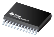
Datasheet Texas Instruments TPS65150QPWPRQ1
| Manufacturer | Texas Instruments |
| Series | TPS65150-Q1 |
| Part Number | TPS65150QPWPRQ1 |

Automotive, compact LCD bias Power Supply with integrated VCOM Buffer 24-HTSSOP -40 to 125
Datasheets
TPS65150-Q1 Automotive LCD Power Supply for Source and Gate Drivers with Gate Voltage Shaping and VCOM Buffer datasheet
PDF, 1.7 Mb, Revision: C, File published: May 26, 2017
Extract from the document
Prices
Status
| Lifecycle Status | Active (Recommended for new designs) |
| Manufacture's Sample Availability | Yes |
Packaging
| Pin | 24 |
| Package Type | PWP |
| Industry STD Term | HTSSOP |
| JEDEC Code | R-PDSO-G |
| Package QTY | 2000 |
| Carrier | LARGE T&R |
| Width (mm) | 4.4 |
| Length (mm) | 7.8 |
| Thickness (mm) | 1 |
| Pitch (mm) | 0.65 |
| Max Height (mm) | 1.2 |
| Mechanical Data | Download |
Parametrics
| DisplayType | Automotive,LCD Unipolar |
| IC Integration | LCD Bias |
| Pin/Package | 24HTSSOP |
| Source Driver Voltage(Max) | 15 V |
| Source Driver Voltage(Min) | 5 V |
| Special Function | Adjustable Sequencing,GPM/GVS,VCOM/OpAmp |
| Target Application | 7 inches or less,7 to 13 inches |
| Topology | Boost |
| Vin(Max) | 6 V |
| Vin(Min) | 1.8 V |
Eco Plan
| RoHS | Compliant |
Design Kits & Evaluation Modules
- Evaluation Modules & Boards: TPS65150EVM-697
TPS65150 Low Vin LCD power supply (bias) with integrated VCOM Evaluation Module
Lifecycle Status: Active (Recommended for new designs)
Application Notes
- How to Calculate the Output Voltage Ranges of the Charge Pumps in the TPS65150PDF, 265 Kb, File published: Feb 6, 2017
This application report tells you how to estimate the output voltage range of the charge pumps in theTPS65150. It assumes that the output current from each charge pump is 25 mA or less.This application report was written specifically for the TPS65150 but the principles in it are applicable toall devices that use the same charge-pump topology. - Understanding Undervoltage Lockout in Power Devices (Rev. A)PDF, 90 Kb, Revision: A, File published: Sep 19, 2018
Many integrated circuits include an undervoltage lockout (UVLO) function to disable the device at low supply voltages. Below the minimum supply voltage the function and performance of a device may be undefined making it impossible to predict system behavior. This application note explains how to correctly understand the undervoltage lockout specification in the data sheets of TI's power products. - Basic Calculation of a Boost Converter's Power Stage (Rev. C)PDF, 186 Kb, Revision: C, File published: Jan 8, 2014
This application note gives the equations to calculate the power stage of a boost converter built with an IC with integrated switch and operating in continuous conduction mode. It is not intended to give details on the functionality of a boost converter (see Reference 1) or how to compensate a converter. See the references at the end of this document if more detail is needed.
Model Line
Series: TPS65150-Q1 (1)
- TPS65150QPWPRQ1
Manufacturer's Classification
- Semiconductors > Power Management > LCD/OLED Display Bias Solutions
