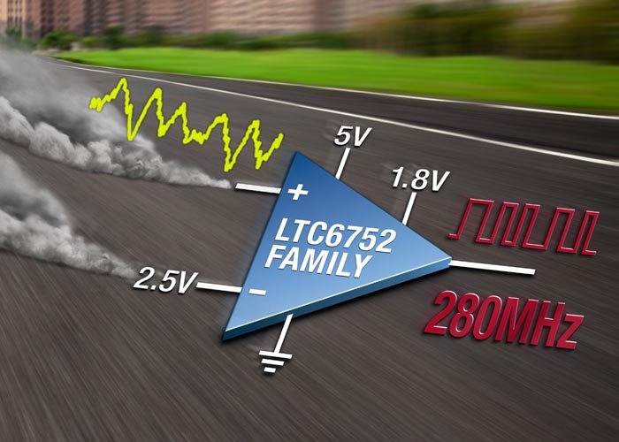
Linear Technology Corporation announces the LTC6752 family of comparators with fast rise and fall times of 1.2 ns and a toggle frequency of 280 MHz, making them the fastest CMOS output comparators available today. Designed for driving logic levels from 3.3 V down to 1.8 V, the LTC6752 exhibits only 2.9 ns of propagation delay and overdrive dispersion of only 1.8 ns. Jitter is only 4.5 ps for a 100 mVpp, 100 MHz sinusoidal input, and the outputs swing to within 200 mV of the rails with up to 8 mA of load current. All of this high speed performance is well suited for a broad range of timing-critical applications, where fast response times and CMOS output levels are required.
The LTC6752 consists of 5 options offered in different packages with unique combinations of features, such as separate input and output supplies, low power shutdown, output latch, adjustable hysteresis and complementary outputs. The latch provides the ability to quickly capture the state of the comparator. With the adjustable hysteresis feature, the default 5 mV hysteresis can be increased up to 40 mV for clean switching in the presence of noisy input signals, and it allows for hysteresis to be completely eliminated. The separate input and output supply allows the output logic level to be independent of the input signal range for translation from one logic level to another. With the shutdown, power can be reduced while enabling the comparator to wake up quickly. In addition, the complementary CMOS outputs simplify logic interfaces and eliminate the need for separate logic inversion.
The inputs for the LTC6752 extend beyond both rails, particularly useful for single supply operation. All members of the LTC6752 family are capable of driving 3.3 V and 2.5 V logic. The LTC6752-2, LTC6752-3 and LTC6752-4 have separate input and output supplies, decoupling the input and output voltage levels and enabling them to drive 1.8 V logic.
The LTC6752 family is offered in the TSOT23, SC70, MSOP8 and a 12-lead 3 mm × 3 mm QFN package. These parts are fully specified over two temperature ranges: –40°C to 85°C and –40 °C to 125 °C. All members of the LTC6752 family are in full production, with prices starting at $1.62 each in 1,000 piece quantities.
|
Part#
|
Adj. Hyst
|
Input & Output
Supplies |
Shutdown
|
Q / Q
Outputs |
Latch
|
Output CMOS
Logic Levels |
Package
|
||
|
3.3 V
|
2.5 V
|
1.8 V
|
|||||||
|
LTC6752
|
•
|
•
|
TSOT-23-5
|
||||||
|
LTC6752-1
|
•
|
•
|
•
|
•
|
SC70-6
|
||||
|
LTC6752-2
|
•
|
•
|
•
|
•
|
•
|
•
|
•
|
MSOP8
|
|
|
LTC6752-3
|
•
|
•
|
•
|
•
|
•
|
•
|
•
|
•
|
3×3 QFN12
|
|
LTC6752-4
|
•
|
•
|
•
|
•
|
SC70-6
|
||||
Summary of Features: LTC6752
- 280 MHz Toggle Rate
- 2.9 ns Low Propagation Delay
- Rail-to-Rail Inputs Extend Beyond Both Rails
- CMOS Outputs Capable of Driving ±22 mA
- 4.5 mA Low Quiescent Current
- Features within the LTC6752 Family:
- 2.45 V to 5.25 V Input Supply & 1.71 V to 3.5 V Output Supply (Separate Supply Option)
- 2.45 V to 3.5 V Supply (Single Supply Option)
- Shutdown Pin for Reduced Power
- Output Latch & Adjustable Hysteresis
- Complementary Outputs
- Packages: TSOT-23, MSOP, SC70, 3 mm × 3 mm QFN
- Operating Temperature Range: –40°C to 125°C
