You can improve a current sink's accuracy by at least two orders of magnitude by adding two standard 1%-tolerance resistors. As a bonus, you also compensate for errors that a low-current-gain pass transistor's base current introduces. To do so, you measure the transistor's base current and add a proportionally scaled error term to the source's reference voltage. When you design a current sink, you can use a MOSFET for the sink's pass transistor because of its nearly infinite power gain and low gate current. However, a high-power MOSFET presents high input and output capacitances that reduce the sink's high-frequency output impedance.
As an alternative, a low-current-gain, bipolar power transistor presents a much lower output capacitance than does a MOSFET of comparable power ratings. Figure 1 shows a design for a bipolar-transistor-based current sink that unfortunately suffers from accuracy errors due to Q1's base current's flowing into the current-measurement resistor R1. The base current varies with changes in Q1's collector current and current gain, which in turn depend on Q1's production tolerances, junction temperature, and collector-emitter voltage.
You can use a Darlington transistor to increase the circuit's current gain and reduce the output error, but few Darlington transistors offer good high-frequency parameters. Superbeta power transistors are rare, have typically lower unity-gain-bandwidth frequencies, and are more expensive. In other words, even though a bipolar transistor presents higher output impedance at high frequencies, the error from its base current makes it a poor choice for a high-precision current sink. You could compensate for base-current errors by measuring the output transistor's collector current and introducing a correction factor, but that approach increases circuit complexity and reduces the sink's output impedance.
 |
|
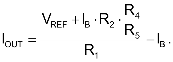
| Figure 1 | This typical quickly responding constant-current sink uses a bipolar transistor but suffers from base-current-induced error. Its normal output current is IOUT = (VREF/R1) – IB. |
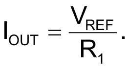
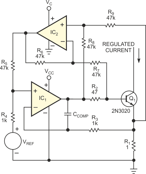
Figure 2 shows a better approach, which adds a differential amplifier, IC2, and resistors R6 through R9 to measure Q1's base current by sampling the voltage across R2. Resistors R4 and R5 scale and sum the error and reference voltages you apply to differential amplifier IC1. Because IC1's inverting input connects to current-shunt resistor R1's upper end and not to ground, the reference voltage, VREF, determines the error voltage applied to Q1, preserving output scaling and allowing output-current calculation as VREF/R1. As a result, the regulated voltage across R1 represents the sum of the desired output current plus the transistor's base current. Because the transistor inherently "subtracts" its base current, its collector current and, hence, the output current have no base-current error.
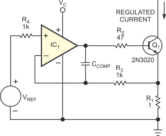
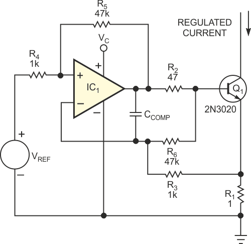
You can simplify the circuit and preserve its error-correction properties by combining IC1 and IC2; better yet, you can add two resistors to Figure 1 to achieve the same effect. Figure 3 shows the final circuit. To understand its operation, think of the circuit as a voltage regulator that delivers a voltage equal to VREF across R1. If you short-circuit base resistor R2, note that any common-mode error that resistors R5 and R6 introduce cancels and thus has no effect on Q1's base voltage. When you feed the voltage drop back to IC1's input through R5 and R4, the voltage drop across R2, representing Q1's base current, increases the regulated voltage across R1 by the ratio of R5/R4. If the ratio of R5/R4 equals that of R2/R1, the voltage across R1 includes an error term that effectively cancels the base current. If R3 = R4 and R5 = R6, the following equation describes the output current, IOUT:
Because the base current, IB, appears twice with opposite signs and cancels, the equation simplifies to:
To optimize the circuit's performance, use the following resistor ratios:
Using standard 1%-tolerance resistors in the circuit of Figure 3 reduces the error from Q1's base current to about one-one-hundredth of its uncompensated level. Without compensation, a low-gain power transistor with a typical current gain of 25 at Q1 would introduce a full-scale current error of 4%. The circuit corrects the error to 0.04% and raises Q1's current gain to an effective current gain of 2500. Perfect matching would result in an immeasurably small base-current error. Note that IC1's input common-mode-voltage range must include the negative-supply-voltage rail. Equal resistances at both of IC1's inputs balance the op amp's input-bias currents. The minimum power-supply voltage depends on IC1's maximum current-sourcing capability and on the sum of the worst-case voltage drops across Q1's base-emitter junction, R1 and R2. The circuit's maximum output current depends on Q1's worst-case minimum current gain times IC1's worst-case minimum output current.
 |
|
| Figure 2 | Adding base-current error compensation improves the circuit’s performance. Using perfectly matched resistors simplifies the output-current equation to IOUT = (VREF/R1). |
To ensure stable operation, use a unity-gain-stable op amp for IC1. When the circuit operates within its nominal current range, an op amp whose response time is substantially longer than Q1's generally doesn't require installation of compensation capacitor CCOMP. However, a small capacitor of a few tens of picofarads guarantees stability under all conditions – for example, when the circuit's output current and the feedback voltage across R1 approach zero.
 |
|
| Figure 3 | You can further simplify the current sink’s design by adding only two resistors, R5 and R6, to the original in Figure 1. The output-current equation remains IOUT = (VREF/R1), as in Figure 2. |
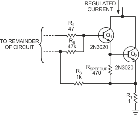
The circuit in Figure 3 works equally well if you use a Darlington transistor for Q1 because its higher current gain further improves the circuit's operation. If you use two discrete bipolar transistors, you can improve the composite Darlington transistor's turn-off time by connecting a resistor between the output transistor's base and emitter to remove its excess base charge (Figure 4).
 |
|
| Figure 4 | Adding RSPEEDUP improves the performance of a two-transistor Darlington output stage. |
You can use either a fixed or an adjustable reference-voltage source, but for the smallest possible error, the reference source's output impedance should be fairly low to sink feedback current from R4. You can also proportionally increase the values of resistors R3 through R6 to reduce the amount of current that the reference source absorbs. It's amazing what you can achieve by adding only two resistors to an already-simple circuit.
