PDF, 640 Kb, Language: en, File uploaded: Aug 26, 2025, Pages: 13
N-Channel General Purpose Amplifier in SOT-23 Package
Extract from the document
G S
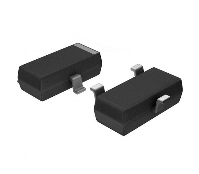
G S TO-92 SOT-23 D NOTE: Source & Drain
are interchangeable D Mark: 62P / 62Q J201 / J202 / MMBFJ201 / MMBFJ202 MMBFJ201
MMBFJ202 J201
J202 N-Channel General Purpose Amplifier
This device is designed primarily for low level audio and general
purpose applications with high impedance signal sources. Sourced
from Process 52. Absolute Maximum Ratings*
Symbol TA = 25°C unless otherwise noted Parameter VDG Drain-Gate Voltage VGS Gate-Source Voltage IGF Forward Gate Current TJ ,Tstg Operating and Storage Junction Temperature Range Value Units 40 V -40 V 50 mA -55 to +150 °C *These ratings are limiting values above which the serviceability of any semiconductor device may be impaired.
NOTES:
1) These ratings are based on a maximum junction temperature of 150 degrees C.
2) These are steady state limits. The factory should be consulted on applications involving pulsed or low duty cycle operations Thermal Characteristics
Symbol
PD TA = 25°C unless otherwise noted Characteristic RθJC Total Device Dissipation
Derate above 25°C
Thermal Resistance, Junction to Case RθJA Thermal Resistance, Junction to Ambient *Device mounted on FR-4 PCB 1.6" X 1.6" X 0.06." 1997 Fairchild Semiconductor Corporation Max Units J202-203
625
5.0
125 *MMBFJ202-203
350
2.8 357 556 mW
mW/°C
°C/W …