Datasheet Texas Instruments CD74ACT08
| Manufacturer | Texas Instruments |
| Series | CD74ACT08 |
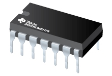
Quad 2-Input AND Gates
Datasheets
Quadruple 2-Input Positive-AND Gates datasheet
PDF, 970 Kb, Revision: B, File published: Jun 12, 2002
Extract from the document
Prices
Status
| CD74ACT08E | CD74ACT08M | CD74ACT08M96 | CD74ACT08M96E4 | CD74ACT08M96G4 | CD74ACT08ME4 | CD74ACT08MG4 | |
|---|---|---|---|---|---|---|---|
| Lifecycle Status | Active (Recommended for new designs) | Active (Recommended for new designs) | Active (Recommended for new designs) | Active (Recommended for new designs) | Active (Recommended for new designs) | Active (Recommended for new designs) | Active (Recommended for new designs) |
| Manufacture's Sample Availability | No | No | No | No | No | No | No |
Packaging
| CD74ACT08E | CD74ACT08M | CD74ACT08M96 | CD74ACT08M96E4 | CD74ACT08M96G4 | CD74ACT08ME4 | CD74ACT08MG4 | |
|---|---|---|---|---|---|---|---|
| N | 1 | 2 | 3 | 4 | 5 | 6 | 7 |
| Pin | 14 | 14 | 14 | 14 | 14 | 14 | 14 |
| Package Type | N | D | D | D | D | D | D |
| Industry STD Term | PDIP | SOIC | SOIC | SOIC | SOIC | SOIC | SOIC |
| JEDEC Code | R-PDIP-T | R-PDSO-G | R-PDSO-G | R-PDSO-G | R-PDSO-G | R-PDSO-G | R-PDSO-G |
| Package QTY | 25 | 50 | 2500 | 2500 | 2500 | 50 | 50 |
| Carrier | TUBE | TUBE | LARGE T&R | LARGE T&R | LARGE T&R | TUBE | TUBE |
| Device Marking | CD74ACT08E | ACT08M | ACT08M | ACT08M | ACT08M | ACT08M | ACT08M |
| Width (mm) | 6.35 | 3.91 | 3.91 | 3.91 | 3.91 | 3.91 | 3.91 |
| Length (mm) | 19.3 | 8.65 | 8.65 | 8.65 | 8.65 | 8.65 | 8.65 |
| Thickness (mm) | 3.9 | 1.58 | 1.58 | 1.58 | 1.58 | 1.58 | 1.58 |
| Pitch (mm) | 2.54 | 1.27 | 1.27 | 1.27 | 1.27 | 1.27 | 1.27 |
| Max Height (mm) | 5.08 | 1.75 | 1.75 | 1.75 | 1.75 | 1.75 | 1.75 |
| Mechanical Data | Download | Download | Download | Download | Download | Download | Download |
Parametrics
| Parameters / Models | CD74ACT08E | CD74ACT08M | CD74ACT08M96 | CD74ACT08M96E4 | CD74ACT08M96G4 | CD74ACT08ME4 | CD74ACT08MG4 |
|---|---|---|---|---|---|---|---|
| Bits | 4 | 4 | 4 | 4 | 4 | 4 | 4 |
| ICC @ Nom Voltage(Max), mA | 0.04 | 0.04 | 0.04 | 0.04 | 0.04 | 0.04 | 0.04 |
| Operating Temperature Range, C | -55 to 125 | -55 to 125 | -55 to 125 | -55 to 125 | -55 to 125 | -55 to 125 | -55 to 125 |
| Output Drive (IOL/IOH)(Max), mA | -24/24 | -24/24 | -24/24 | -24/24 | -24/24 | -24/24 | -24/24 |
| Package Group | PDIP | SOIC | SOIC | SOIC | SOIC | SOIC | SOIC |
| Package Size: mm2:W x L, PKG | See datasheet (PDIP) | 14SOIC: 52 mm2: 6 x 8.65(SOIC) | 14SOIC: 52 mm2: 6 x 8.65(SOIC) | 14SOIC: 52 mm2: 6 x 8.65(SOIC) | 14SOIC: 52 mm2: 6 x 8.65(SOIC) | 14SOIC: 52 mm2: 6 x 8.65(SOIC) | 14SOIC: 52 mm2: 6 x 8.65(SOIC) |
| Rating | Catalog | Catalog | Catalog | Catalog | Catalog | Catalog | Catalog |
| Schmitt Trigger | No | No | No | No | No | No | No |
| Technology Family | ACT | ACT | ACT | ACT | ACT | ACT | ACT |
| VCC(Max), V | 5.5 | 5.5 | 5.5 | 5.5 | 5.5 | 5.5 | 5.5 |
| VCC(Min), V | 4.5 | 4.5 | 4.5 | 4.5 | 4.5 | 4.5 | 4.5 |
| Voltage(Nom), V | 5 | 5 | 5 | 5 | 5 | 5 | 5 |
| tpd @ Nom Voltage(Max), ns | 11.7 | 11.7 | 11.7 | 11.7 | 11.7 | 11.7 | 11.7 |
Eco Plan
| CD74ACT08E | CD74ACT08M | CD74ACT08M96 | CD74ACT08M96E4 | CD74ACT08M96G4 | CD74ACT08ME4 | CD74ACT08MG4 | |
|---|---|---|---|---|---|---|---|
| RoHS | Compliant | Compliant | Compliant | Compliant | Compliant | Compliant | Compliant |
| Pb Free | Yes |
Application Notes
- Selecting the Right Level Translation Solution (Rev. A)PDF, 313 Kb, Revision: A, File published: Jun 22, 2004
Supply voltages continue to migrate to lower nodes to support today's low-power high-performance applications. While some devices are capable of running at lower supply nodes others might not have this capability. To haveswitching compatibility between these devices the output of each driver must be compliant with the input of the receiver that it is driving. There are several level-translati - Using High Speed CMOS and Advanced CMOS in Systems With Multiple VccPDF, 43 Kb, File published: Apr 1, 1996
Though low power consumption is a feature of CMOS devices sometimes this feature does not meet a designer?s system power supply constraints. Therefore a partial system power down or multiple Vcc supplies are used to meet the needs of the system. This document shows electrostatic discharge protection circuits. It also provides circuit and bus driver examples of partial system power down and curren
Model Line
Series: CD74ACT08 (7)
Manufacturer's Classification
- Semiconductors> Logic> Gate> AND Gate
