Datasheet Texas Instruments SN74AUP1G99
| Manufacturer | Texas Instruments |
| Series | SN74AUP1G99 |
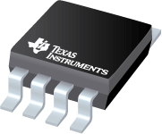
Low-Power Ultra-Configurable Multiple-Function Gate with 3-State Outputs
Datasheets
Low-Power Ultra-Configurable Multiple-Function Gate With 3-State Outputs datasheet
PDF, 1.0 Mb, Revision: C, File published: Jul 9, 2007
Extract from the document
Status
| SN74AUP1G99DCTR | SN74AUP1G99DCTT | SN74AUP1G99DCUR | SN74AUP1G99DCUT | SN74AUP1G99DCUTE4 | SN74AUP1G99YZPR | |
|---|---|---|---|---|---|---|
| Lifecycle Status | Active (Recommended for new designs) | Active (Recommended for new designs) | Active (Recommended for new designs) | Active (Recommended for new designs) | Active (Recommended for new designs) | Active (Recommended for new designs) |
| Manufacture's Sample Availability | Yes | Yes | No | No | No | Yes |
Packaging
| SN74AUP1G99DCTR | SN74AUP1G99DCTT | SN74AUP1G99DCUR | SN74AUP1G99DCUT | SN74AUP1G99DCUTE4 | SN74AUP1G99YZPR | |
|---|---|---|---|---|---|---|
| N | 1 | 2 | 3 | 4 | 5 | 6 |
| Pin | 8 | 8 | 8 | 8 | 8 | 8 |
| Package Type | DCT | DCT | DCU | DCU | DCU | YZP |
| Industry STD Term | SSOP | SSOP | VSSOP | VSSOP | VSSOP | DSBGA |
| JEDEC Code | R-PDSO-G | R-PDSO-G | R-PDSO-G | R-PDSO-G | R-PDSO-G | R-XBGA-N |
| Package QTY | 3000 | 250 | 3000 | 250 | 3000 | |
| Carrier | LARGE T&R | SMALL T&R | LARGE T&R | SMALL T&R | LARGE T&R | |
| Device Marking | Z | Z | H99Q | H99Q | HYN | |
| Width (mm) | 2.8 | 2.8 | 2 | 2 | 2 | 2.25 |
| Length (mm) | 2.95 | 2.95 | 2.3 | 2.3 | 2.3 | 1.25 |
| Thickness (mm) | 1.29 | 1.29 | .85 | .85 | .85 | .31 |
| Pitch (mm) | .65 | .65 | .5 | .5 | .5 | .5 |
| Max Height (mm) | 1.3 | 1.3 | .9 | .9 | .9 | .5 |
| Mechanical Data | Download | Download | Download | Download | Download | Download |
Parametrics
| Parameters / Models | SN74AUP1G99DCTR | SN74AUP1G99DCTT | SN74AUP1G99DCUR | SN74AUP1G99DCUT | SN74AUP1G99DCUTE4 | SN74AUP1G99YZPR |
|---|---|---|---|---|---|---|
| 3-State Output | Yes | Yes | Yes | Yes | Yes | Yes |
| Approx. Price (US$) | 0.14 | 1ku | |||||
| Bits | 1 | 1 | 1 | 1 | 1 | |
| Bits(#) | 1 | |||||
| F @ Nom Voltage(Max), Mhz | 100 | 100 | 100 | 100 | 100 | |
| F @ Nom Voltage(Max)(Mhz) | 100 | |||||
| Gate Type | CONFIGURABLE | CONFIGURABLE | CONFIGURABLE | CONFIGURABLE | CONFIGURABLE | CONFIGURABLE |
| ICC @ Nom Voltage(Max), mA | 0.0009 | 0.0009 | 0.0009 | 0.0009 | 0.0009 | |
| ICC @ Nom Voltage(Max)(mA) | 0.0009 | |||||
| Logic | True | True | True | True | True | True |
| Operating Temperature Range, C | -40 to 85 | -40 to 85 | -40 to 85 | -40 to 85 | -40 to 85 | |
| Operating Temperature Range(C) | -40 to 85 | |||||
| Output Drive (IOL/IOH)(Max), mA | 4/-4 | 4/-4 | 4/-4 | 4/-4 | 4/-4 | |
| Output Drive (IOL/IOH)(Max)(mA) | 4/-4 | |||||
| Package Group | SM8 | SM8 | VSSOP | VSSOP | VSSOP | DSBGA |
| Package Size: mm2:W x L, PKG | 8SM8: 12 mm2: 4 x 2.95(SM8) | 8SM8: 12 mm2: 4 x 2.95(SM8) | 8VSSOP: 6 mm2: 3.1 x 2(VSSOP) | 8VSSOP: 6 mm2: 3.1 x 2(VSSOP) | See datasheet (DSBGA) | |
| Package Size: mm2:W x L (PKG) | See datasheet (DSBGA) | |||||
| Rating | Catalog | Catalog | Catalog | Catalog | Catalog | Catalog |
| Schmitt Trigger | Yes | Yes | Yes | Yes | Yes | Yes |
| Special Features | IOFF,low power consumption,low tpd,Schmitt-trigger,Configurable | IOFF,low power consumption,low tpd,Schmitt-trigger,Configurable | IOFF,low power consumption,low tpd,Schmitt-trigger,Configurable | IOFF,low power consumption,low tpd,Schmitt-trigger,Configurable | IOFF low power consumption low tpd Schmitt-trigger Configurable | IOFF,low power consumption,low tpd,Schmitt-trigger,Configurable |
| Sub-Family | Configurable Logic | Configurable Logic | Configurable Logic | Configurable Logic | Configurable Logic | Configurable Logic |
| Technology Family | AUP | AUP | AUP | AUP | AUP | AUP |
| VCC(Max), V | 3.6 | 3.6 | 3.6 | 3.6 | 3.6 | |
| VCC(Max)(V) | 3.6 | |||||
| VCC(Min), V | 0.8 | 0.8 | 0.8 | 0.8 | 0.8 | |
| VCC(Min)(V) | 0.8 | |||||
| Voltage(Nom), V | 0.8,1.2,1.5,1.8,2.5,3.3 | 0.8,1.2,1.5,1.8,2.5,3.3 | 0.8,1.2,1.5,1.8,2.5,3.3 | 0.8,1.2,1.5,1.8,2.5,3.3 | 0.8,1.2,1.5,1.8,2.5,3.3 | |
| Voltage(Nom)(V) | 0.8 1.2 1.5 1.8 2.5 3.3 | |||||
| tpd @ Nom Voltage(Max), ns | 48,24.9,15.1,11.7,7.9,6.7 | 48,24.9,15.1,11.7,7.9,6.7 | 48,24.9,15.1,11.7,7.9,6.7 | 48,24.9,15.1,11.7,7.9,6.7 | 48,24.9,15.1,11.7,7.9,6.7 | |
| tpd @ Nom Voltage(Max)(ns) | 48 24.9 15.1 11.7 7.9 6.7 |
Eco Plan
| SN74AUP1G99DCTR | SN74AUP1G99DCTT | SN74AUP1G99DCUR | SN74AUP1G99DCUT | SN74AUP1G99DCUTE4 | SN74AUP1G99YZPR | |
|---|---|---|---|---|---|---|
| RoHS | Compliant | Compliant | Compliant | Compliant | Not Compliant | Compliant |
| Pb Free | No |
Application Notes
- Understanding Schmitt TriggersPDF, 80 Kb, File published: Sep 21, 2011
Model Line
Series: SN74AUP1G99 (6)
Manufacturer's Classification
- Semiconductors> Logic> Little Logic