Datasheet Texas Instruments SN74AUP2G126
| Manufacturer | Texas Instruments |
| Series | SN74AUP2G126 |
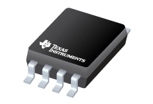
Low-Power Dual Bus Buffer Gate With 3-State Outputs
Datasheets
SN74AUP2G126 Low-Power Dual Bus Buffer Gate With 3-State Outputs datasheet
PDF, 1.4 Mb, Revision: D, File published: Dec 30, 2009
Extract from the document
Status
| SN74AUP2G126DCUR | SN74AUP2G126DQER | SN74AUP2G126RSER | SN74AUP2G126YFPR | SN74AUP2G126YZPR | |
|---|---|---|---|---|---|
| Lifecycle Status | Active (Recommended for new designs) | Active (Recommended for new designs) | Active (Recommended for new designs) | Active (Recommended for new designs) | Active (Recommended for new designs) |
| Manufacture's Sample Availability | Yes | Yes | Yes | Yes | Yes |
Packaging
| SN74AUP2G126DCUR | SN74AUP2G126DQER | SN74AUP2G126RSER | SN74AUP2G126YFPR | SN74AUP2G126YZPR | |
|---|---|---|---|---|---|
| N | 1 | 2 | 3 | 4 | 5 |
| Pin | 8 | 8 | 8 | 8 | 8 |
| Package Type | DCU | DQE | RSE | YFP | YZP |
| Industry STD Term | VSSOP | X2SON | UQFN | DSBGA | DSBGA |
| JEDEC Code | R-PDSO-G | R-PSSO-N | S-PQFP-N | R-XBGA-N | R-XBGA-N |
| Package QTY | 3000 | 5000 | 5000 | 3000 | 3000 |
| Carrier | LARGE T&R | LARGE T&R | LARGE T&R | LARGE T&R | LARGE T&R |
| Device Marking | H26R | PW | PW | HNN | HNN |
| Width (mm) | 2 | 1 | 1.5 | 2.25 | |
| Length (mm) | 2.3 | 1.4 | 1.5 | 1.25 | |
| Thickness (mm) | .85 | .37 | .55 | .31 | |
| Pitch (mm) | .5 | .35 | .5 | .4 | .5 |
| Max Height (mm) | .9 | .4 | .6 | .5 | .5 |
| Mechanical Data | Download | Download | Download | Download | Download |
Parametrics
| Parameters / Models | SN74AUP2G126DCUR | SN74AUP2G126DQER | SN74AUP2G126RSER | SN74AUP2G126YFPR | SN74AUP2G126YZPR |
|---|---|---|---|---|---|
| 3-State Output | Yes | Yes | Yes | Yes | Yes |
| Bits | 2 | 2 | 2 | 2 | 2 |
| F @ Nom Voltage(Max), Mhz | 100 | 100 | 100 | 100 | 100 |
| Gate Type | BUFFER | BUFFER | BUFFER | BUFFER | BUFFER |
| ICC @ Nom Voltage(Max), mA | 0.0009 | 0.0009 | 0.0009 | 0.0009 | 0.0009 |
| Logic | True | True | True | True | True |
| Operating Temperature Range, C | -40 to 85 | -40 to 85 | -40 to 85 | -40 to 85 | -40 to 85 |
| Output Drive (IOL/IOH)(Max), mA | 4/-4 | 4/-4 | 4/-4 | 4/-4 | 4/-4 |
| Package Group | VSSOP | X2SON | UQFN | DSBGA | DSBGA |
| Package Size: mm2:W x L, PKG | 8VSSOP: 6 mm2: 3.1 x 2(VSSOP) | 8X2SON: 1 mm2: 1 x 1.4(X2SON) | 8UQFN: 2 mm2: 1.5 x 1.5(UQFN) | See datasheet (DSBGA) | See datasheet (DSBGA) |
| Rating | Catalog | Catalog | Catalog | Catalog | Catalog |
| Schmitt Trigger | No | No | No | No | No |
| Special Features | IOFF,low power consumption,low tpd,3-state | IOFF,low power consumption,low tpd,3-state | IOFF,low power consumption,low tpd,3-state | IOFF,low power consumption,low tpd,3-state | IOFF,low power consumption,low tpd,3-state |
| Sub-Family | Non-Inverting Buffer/Driver | Non-Inverting Buffer/Driver | Non-Inverting Buffer/Driver | Non-Inverting Buffer/Driver | Non-Inverting Buffer/Driver |
| Technology Family | AUP | AUP | AUP | AUP | AUP |
| VCC(Max), V | 3.6 | 3.6 | 3.6 | 3.6 | 3.6 |
| VCC(Min), V | 0.8 | 0.8 | 0.8 | 0.8 | 0.8 |
| Voltage(Nom), V | 0.8,1.2,1.5,1.8,2.5,3.3 | 0.8,1.2,1.5,1.8,2.5,3.3 | 0.8,1.2,1.5,1.8,2.5,3.3 | 0.8,1.2,1.5,1.8,2.5,3.3 | 0.8,1.2,1.5,1.8,2.5,3.3 |
| tpd @ Nom Voltage(Max), ns | 36.4,30.8,18,13.6,8.6,7.9 | 36.4,30.8,18,13.6,8.6,7.9 | 36.4,30.8,18,13.6,8.6,7.9 | 36.4,30.8,18,13.6,8.6,7.9 | 36.4,30.8,18,13.6,8.6,7.9 |
Eco Plan
| SN74AUP2G126DCUR | SN74AUP2G126DQER | SN74AUP2G126RSER | SN74AUP2G126YFPR | SN74AUP2G126YZPR | |
|---|---|---|---|---|---|
| RoHS | Compliant | Compliant | Compliant | Compliant | Compliant |
Application Notes
- Understanding Schmitt TriggersPDF, 80 Kb, File published: Sep 21, 2011
Model Line
Series: SN74AUP2G126 (5)
Manufacturer's Classification
- Semiconductors> Logic> Little Logic